PIC12F683
9.4
Effects of Reset
A device Reset forces all registers to their Reset state.
Thus, the A/D module is turned off and any pending
conversion is aborted. The ADRESH:ADRESL
registers are unchanged.
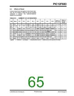
TABLE 9-2:
SUMMARY OF A/D REGISTERS
Value on
Value on:
POR, BOD
Addr Name
Bit 7
Bit 6
Bit 5
Bit 4
Bit 3
Bit 2
Bit 1
Bit 0
all other
Resets
05h
GPIO
—
—
GP5
T0IE
GP4
GP3
GP2
T0IF
GP1
GP0
--xx xxxx --uu uuuu
0000 0000 0000 0000
0Bh/ INTCON
8Bh
GIE
PEIE
INTE
GPIE
INTF
GPIF
0Ch PIR1
EEIF
ADIF
CCP1IF
—
CMIF
OSFIF
TMR2IF
TMR1IF 000- 0000 000- 0000
1Eh
1Fh
85h
ADRESH Most Significant 8 bits of the left shifted A/D result or 2 bits of the right shifted result
xxxx xxxx uuuu uuuu
ADCON0 ADFM
VCFG
—
—
—
CHS1
TRISIO5 TRISIO4 TRISIO3 TRISIO2 TRISIO1 TRISIO0 --11 1111 --11 1111
CCPIE CMIE OSFIE TMR2IE TMR1IE 000- 0000 000- 0000
CHS0
GO/DONE ADON 00-- 0000 00-- 0000
TRISIO
—
8Ch PIE1
EEIE
ADIE
—
9Eh
9Fh
ADRESL Least Significant 2 bits of the left shifted A/D result or 8 bits of the right shifted result
ANSEL ADCS2 ADCS1 ADCS0 ANS3 ANS2 ANS1
xxxx xxxx uuuu uuuu
—
ANS0 -000 1111 -000 1111
Legend:
x= unknown, u= unchanged, — = unimplemented read as ‘0’. Shaded cells are not used for A/D module.
2004 Microchip Technology Inc.
Preliminary
DS41211B-page 63

 MICROCHIP [ MICROCHIP ]