PIC12F683
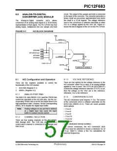
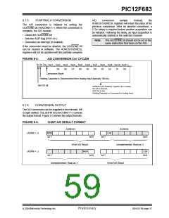
circuit. The output of the sample and hold is connected
to the input of the converter. The converter generates a
binary result via successive approximation and stores
the result in a 10-bit register. The voltage reference
used in the conversion is software selectable to either
VDD or a voltage applied by the VREF pin. Figure 9-1
shows the block diagram of the A/D on the PIC12F683.
9.0
ANALOG-TO-DIGITAL
CONVERTER (A/D) MODULE
The Analog-to-Digital converter (A/D) allows
conversion of an analog input signal to a 10-bit binary
representation of that signal. The PIC12F683 has four
analog inputs, multiplexed into one sample and hold
FIGURE 9-1:
A/D BLOCK DIAGRAM
VDD
VCFG = 0
VCFG = 1
VREF
GP0/AN0
GP1/AN1/VREF
A/D
GP2/AN2
GP4/AN3
10
10
GO/DONE
ADFM
CHS<1:0>
ADON
ADRESH ADRESL
VSS
9.1.3
VOLTAGE REFERENCE
9.1
A/D Configuration and Operation
There are two options for the voltage reference to the
A/D converter: either VDD is used, or an analog voltage
applied to VREF is used. The VCFG bit (ADCON0<6>)
controls the voltage reference selection. If VCFG is set,
then the voltage on the VREF pin is the reference;
otherwise, VDD is the reference.
There are two registers available to control the
functionality of the A/D module:
1. ADCON0 (Register 9-1)
2. ANSEL (Register 9-2)
9.1.1
ANALOG PORT PINS
9.1.4
CONVERSION CLOCK
The ANS<3:0> bits (ANSEL<3:0>) and the TRISIO bits
control the operation of the A/D port pins. Set the cor-
responding TRISIO bits to set the pin output driver to its
high-impedance state. Likewise, set the corresponding
ANSEL bit to disable the digital input buffer.
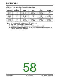
The A/D conversion cycle requires 11 TAD. The source
of the conversion clock is software selectable via the
ADCS bits (ANSEL<6:4>). There are seven possible
clock options:
Note:
Analog voltages on any pin that is defined
as a digital input may cause the input
buffer to conduct excess current.
• FOSC/2
• FOSC/4
• FOSC/8
• FOSC/16
9.1.2
CHANNEL SELECTION
• FOSC/32
There are four analog channels on the PIC12F683,
AN0 through AN3. The CHS bits (ADCON0<3:2>)
control which channel is connected to the sample and
hold circuit.
• FOSC/64
• FRC (dedicated internal oscillator)
For correct conversion, the A/D conversion clock
(1/TAD) must be selected to ensure a minimum TAD of
1.6 µs. Table 9-1 shows a few TAD calculations for
selected frequencies.
2004 Microchip Technology Inc.
Preliminary
DS41211B-page 55

 MICROCHIP [ MICROCHIP ]