PIC12F683
8.6.2
VOLTAGE REFERENCE
ACCURACY/ERROR
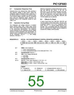
8.6
Comparator Reference
The comparator module also allows the selection of an
internally generated voltage reference for one of the
comparator inputs. The VRCON register, Register 8-3,
controls the voltage reference module shown in
Figure 8-5.
The full range of VSS to VDD cannot be realized due to the
construction of the module. The transistors on the top
and bottom of the resistor ladder network (Figure 8-5)
keep CVREF from approaching VSS or VDD. The excep-
tion is when the module is disabled by clearing the VREN
bit (VRCON<7>). When disabled, the reference voltage
is VSS when VR<3:0> is ‘0000’ and the VRR
(VRCON<5>) bit is set. This allows the comparator to
detect a zero-crossing and not consume CVREF module
current.
8.6.1
CONFIGURING THE VOLTAGE
REFERENCE
The voltage reference can output 32 distinct voltage
levels, 16 in a high range and 16 in a low range.
The following equation determines the output voltages:
The voltage reference is VDD derived and therefore, the
CVREF output changes with fluctuations in VDD. The
tested absolute accuracy of the comparator voltage
reference can be found in Section 15.0 “Electrical
Specifications”.
EQUATION 8-1:
VRR = 1 (Low Range): CVREF = (VR3:VR0/24) x VDD
VRR = 0 (High Range):
CVREF = (VDD/4) + (VR3:VR0 X VDD/32)
FIGURE 8-5:
COMPARATOR VOLTAGE REFERENCE BLOCK DIAGRAM
16 Stages
8R
R
R
R
R
VDD
VRR
8R
16-1 Analog
MUX
VREN
CVREF to
Comparator
Input
VR<3:0>
VREN
VR<3:0> = 0000
VRR
DS41211B-page 52
Preliminary
2004 Microchip Technology Inc.

 MICROCHIP [ MICROCHIP ]