PIC12F683
While the comparator is enabled during Sleep, an inter-
rupt will wake-up the device. If the GIE bit
(INTCON<7>) is set, the device will jump to the inter-
rupt vector (0004h) and if clear, continues execution
with the next instruction. If the device wakes up from
Sleep, the contents of the CMCON0, CMCON1 and
VRCON registers are not affected.
8.7
Comparator Response Time
Response time is the minimum time, after selecting a
new reference voltage or input source, before the
comparator output is ensured to have a valid level. If
the internal reference is changed, the maximum delay
of the internal voltage reference must be considered
when using the comparator output. Otherwise, the
maximum delay of the comparator should be used
(Table 15-8).
8.9
Effects of a Reset
A device Reset forces the CMCON0, CMCON1 and
VRCON registers to their Reset states. This forces the
comparator module to be in the Comparator Reset
mode, CM<2:0> = 000and the voltage reference to its
off state. Thus, all potential inputs are analog inputs
with the comparator and voltage reference disabled to
consume the smallest current possible.
8.8
Operation During Sleep
The comparator and voltage reference, if enabled
before entering Sleep mode, remain active during
Sleep. This results in higher Sleep currents than shown
in the power-down specifications. The additional
current consumed by the comparator and the voltage
reference is shown separately in the specifications. To
minimize power consumption while in Sleep mode, turn
off the comparator, CM<2:0> = 111 and voltage
reference, VRCON<7> = 0.
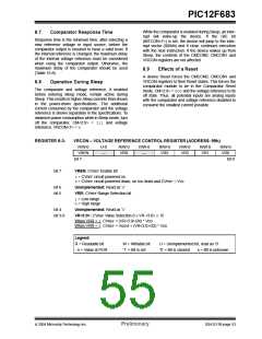
REGISTER 8-3:
VRCON – VOLTAGE REFERENCE CONTROL REGISTER (ADDRESS: 99h)
R/W-0
VREN
U-0
—
R/W-0
VRR
R/W-0
—
R/W-0
VR3
R/W-0
VR2
R/W-0
VR1
R/W-0
VR0
bit 7
bit 0
bit 7
VREN: CVREF Enable bit
1= CVREF circuit powered on
0= CVREF circuit powered down, no IDD drain and CVREF = VSS
bit 6
bit 5
Unimplemented: Read as ‘0’
VRR: CVREF Range Selection bit
1= Low range
0= High range
bit 4
Unimplemented: Read as ‘0’
bit 3-0
VR<3:0>: CVREF Value Selection 0 ≤ VR <3:0> ≤ 15
When VRR = 1: CVREF = (VR<3:0>/24) * VDD
When VRR = 0: CVREF = VDD/4 + (VR<3:0>/32) * VDD
Legend:
R = Readable bit
W = Writable bit
‘1’ = Bit is set
U = Unimplemented bit, read as ‘0’
‘0’ = Bit is cleared x = Bit is unknown
- n = Value at POR
2004 Microchip Technology Inc.
Preliminary
DS41211B-page 53

 MICROCHIP [ MICROCHIP ]