PIC12F683
FIGURE 8-4:
COMPARATOR OUTPUT BLOCK DIAGRAM
CINV
CMSYNC
0
To TMR1
To COUT pin
1
Q
Q
D
TMR1
Clock Source
EN
(1)
To Data Bus
D
Q3
EN
Q
RD CMCON
Set CMIF bit
D
RD CMCON
EN
CL
Reset
Note 1: Comparator output is latched on falling edge of T1 clock source.
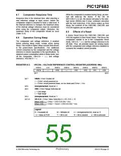
REGISTER 8-2:
CMCON1 – COMPARATOR CONTROL REGISTER 1 (ADDRESS: 1Ah)
U-0
—
U-0
—
U-0
—
U-0
—
U-0
—
U-0
—
R/W-1
R/W-0
T1GSS CMSYNC
bit 0
bit 7
bit 7-2:
bit 1
Unimplemented: Read as ‘0’
T1GSS: Timer1 Gate Source Select bit
1= Timer1 gate source is T1G pin (GP4 must be configured as digital input)
0= Timer1 gate source is comparator output
bit 0
CMSYNC: Comparator Synchronize bit
1= COUT output synchronized with falling edge of Timer1 clock
0= COUT output not synchronized with Timer1 clock
Legend:
R = Readable bit
W = Writable bit
‘1’ = Bit is set
U = Unimplemented bit, read as ‘0’
‘0’ = Bit is cleared x = Bit is unknown
- n = Value at POR
DS41211B-page 50
Preliminary
2004 Microchip Technology Inc.

 MICROCHIP [ MICROCHIP ]