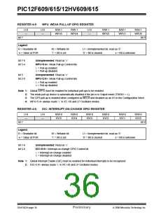
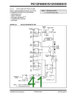
PIC12F609/615/12HV609/615
(1, 2)
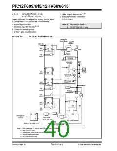
GP4/AN3(1)/CIN1-/T1G/
P1B(1, 2)/OSC2/CLKOUT
• PWM output, alternate pin
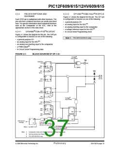
4.2.4.5
• a crystal/resonator connection
• a clock output
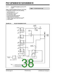
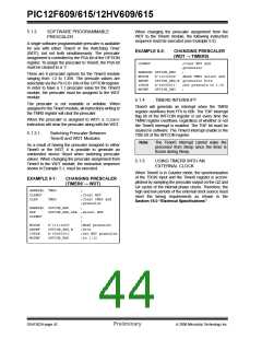
Figure 4-4 shows the diagram for this pin. The GP4 pin
is configurable to function as one of the following:
• a general purpose I/O
Note 1: Alternate pin function.
2: PIC12F615/HV615 only.
(1, 2)
• an analog input for the ADC
• Comparator inverting input
• a Timer1 gate (count enable)
FIGURE 4-4:
BLOCK DIAGRAM OF GP4
(3)
Analog
Input Mode
(1)
CLK
Modes
Data Bus
D
Q
Q
VDD
WR
WPU
CK
Weak
GPPU
RD
WPU
Oscillator
Circuit
OSC1
VDD
CLKOUT
Enable
FOSC/4
1
0
D
Q
Q
I/O Pin
WR
CK
GPIO
CLKOUT
Enable
VSS
D
Q
Q
INTOSC/
(2)
RC/EC
WR
TRISIO
CK
CLKOUT
Enable
RD
TRISIO
Analog
Input Mode
RD
GPIO
D
Q
Q
Q
D
D
CK
WR
IOC
Q1
EN
RD
IOC
Q
(4)
EN
Q
S
Interrupt-on-
Change
From other
GP<5, 3:0> pins
R
RD GPIO
To T1G
To A/D Converter
Write ‘0’ to GBIF
(5)
Note 1: CLK modes are XT, HS, LP, TMR1 LP and CLKOUT Enable.
2: With CLKOUT option.
3: Analog Input mode comes from ANSEL.
4: Set has priority over Reset.
5: PIC12F615/HV615 only.
DS41302A-page 38
Preliminary
© 2006 Microchip Technology Inc.

 MICROCHIP [ MICROCHIP ]