PIC12F609/615/12HV609/615
2.2
Data Memory Organization
2.0
2.1
MEMORY ORGANIZATION
Program Memory Organization
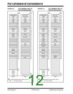
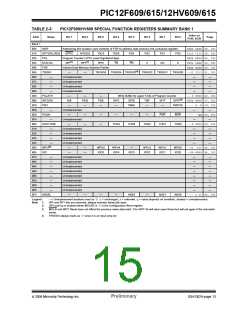
The data memory (see Figure 2-2) is partitioned into two
banks, which contain the General Purpose Registers
(GPR) and the Special Function Registers (SFR). The
Special Function Registers are located in the first 32
locations of each bank. Register locations 40h-7Fh in
Bank 0 are General Purpose Registers, implemented as
static RAM. Register locations F0h-FFh in Bank 1 point
to addresses 70h-7Fh in Bank 0. All other RAM is
unimplemented and returns ‘0’ when read. The RP0 bit
of the STATUS register is the bank select bit.
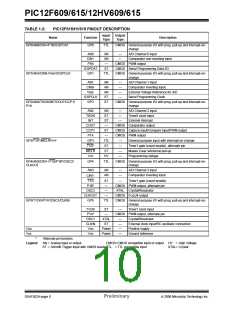
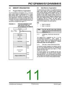
The PIC12F609/615/12HV609/615 has a 13-bit pro-
gram counter capable of addressing an 8K x 14 pro-
gram memory space. Only the first 1K x 14 (0000h-
03FFh) for the PIC12F609/615/12HV609/615 is physi-
cally implemented. Accessing a location above these
boundaries will cause a wraparound within the first 1K
x 14 space. The Reset vector is at 0000h and the inter-
rupt vector is at 0004h (see Figure 2-1).
RP0
FIGURE 2-1:
PROGRAM MEMORY MAP
AND STACK FOR THE
PIC12F609/615/12HV609/615
0
1
→
→
Bank 0 is selected
Bank 1 is selected
PC<12:0>
13
Note:
The IRP and RP1 bits of the STATUS
register are reserved and should always be
maintained as ‘0’s.
CALL, RETURN
RETFIE, RETLW
Stack Level 1
Stack Level 2
2.2.1
GENERAL PURPOSE REGISTER
FILE
The register file is organized as 64 x 8 in the
PIC12F609/615/12HV609/615. Each register is
accessed, either directly or indirectly, through the File
Select Register (FSR) (see Section 2.4 “Indirect
Addressing, INDF and FSR Registers”).
Stack Level 8
Reset Vector
0000h
2.2.2
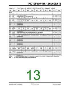
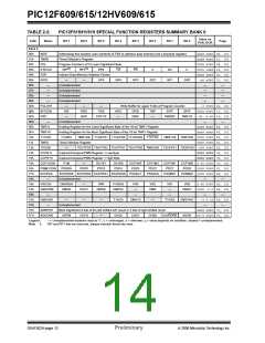
SPECIAL FUNCTION REGISTERS
Interrupt Vector
0004h
The Special Function Registers are registers used by
the CPU and peripheral functions for controlling the
desired operation of the device (see Table 2-1). These
registers are static RAM.
0005h
On-chip Program
Memory
The special registers can be classified into two sets:
core and peripheral. The Special Function Registers
associated with the “core” are described in this section.
Those related to the operation of the peripheral features
are described in the section of that peripheral feature.
03FFh
0400h
Wraps to 0000h-07FFh
1FFFh
© 2006 Microchip Technology Inc.
Preliminary
DS41302A-page 9

 MICROCHIP [ MICROCHIP ]