PIC12F609/615/12HV609/615
Block Diagrams and pinout descriptions of the devices
are as follows:
1.0
DEVICE OVERVIEW
The PIC12F609/615/12HV609/615 devices are covered
by this data sheet. They are available in 8-pin PDIP,
SOIC, TSSOP and DFN packages.
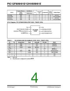
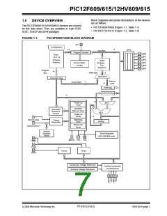
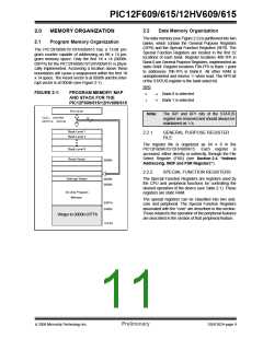
• PIC12F609/HV609 (Figure 1-1, Table 1-1)
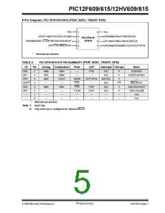
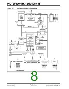
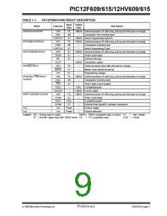
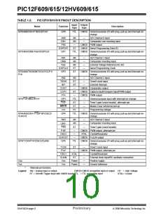
• PIC12F615/HV615 (Figure 1-2, Table 1-2)
FIGURE 1-1:
PIC12F609/HV609 BLOCK DIAGRAM
INT
Configuration
13
8
GPIO
Data Bus
Program Counter
GP0
GP1
GP2
GP3
GP4
GP5
Flash
1K X 14
Program
Memory
RAM
64 Bytes
File
Registers
8-Level Stack
(13-Bit)
Program
Bus
14
RAM Addr
9
Addr MUX
Instruction Reg
Indirect
Addr
7
Direct Addr
8
FSR Reg
STATUS Reg
8
3
Power-up
Timer
MUX
Oscillator
Start-up Timer
Instruction
Decode &
Control
ALU
Power-on
Reset
8
Watchdog
Timer
OSC1/CLKIN
Timing
Generation
W Reg
Brown-out
Reset
OSC2/CLKOUT
Internal
Oscillator
Block
Shunt Regulator
(PIC12HV609 only)
VDD
VSS
MCLR
T1G
T1CKI
T0CKI
Timer0
Timer1
Comparator Voltage Reference
Absolute Voltage Reference
Analog Comparator
and Reference
© 2006 Microchip Technology Inc.
Preliminary
DS41302A-page 5

 MICROCHIP [ MICROCHIP ]