PIC12(L)F1501
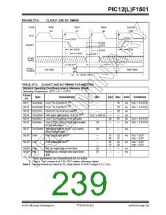
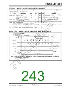
TABLE 27-7: PIC12(L)F1501 A/D CONVERSION REQUIREMENTS
Standard Operating Conditions (unless otherwise stated)
Operating temperature
-40°C TA +125°C
Param
Sym.
No.
Characteristic
Min.
Typ†
Max. Units
Conditions
AD130* TAD
A/D Clock Period
1.0
1.0
—
9.0
6.0
s
s
TOSC-based
A/D Internal FRC Oscillator
Period
1.6
ADCS<1:0> = 11(ADFRC mode)
AD131 TCNV Conversion Time (not including
Acquisition Time)(1)
—
—
11
—
—
TAD Set GO/DONE bit to conversion
complete
AD132* TACQ Acquisition Time
5.0
s
*
These parameters are characterized but not tested.
†
Data in “Typ” column is at 3.0V, 25°C unless otherwise stated. These parameters are for design guidance only and are not
tested.
Note 1: The ADRES register may be read on the following TCY cycle.
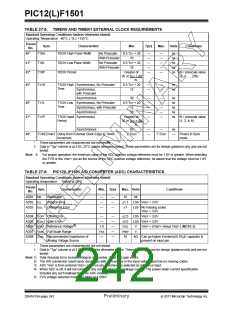
FIGURE 27-10:
PIC12(L)F1501 A/D CONVERSION TIMING (NORMAL MODE)
BSF ADCON0, GO
1 TCY
AD134
Q4
(TOSC/2(1)
)
AD131
AD130
A/D CLK
9
8
7
6
3
2
1
0
A/D Data
ADRES
NEW_DATA
1 TCY
OLD_DATA
ADIF
GO
DONE
Sampling Stopped
AD132
Sample
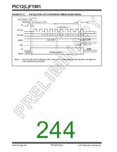
Note 1: If the A/D clock source is selected as FRC, a time of TCY is added before the A/D clock starts. This allows the
SLEEPinstruction to be executed.
2011 Microchip Technology Inc.
Preliminary
DS41615A-page 243

 MICROCHIP [ MICROCHIP ]