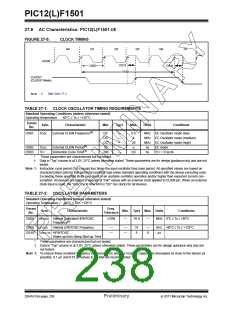
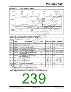
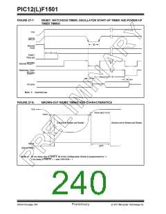
PIC12(L)F1501
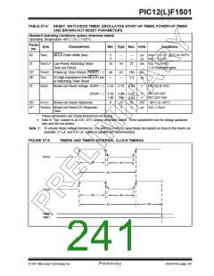
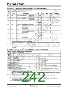
TABLE 27-5: TIMER0 AND TIMER1 EXTERNAL CLOCK REQUIREMENTS
Standard Operating Conditions (unless otherwise stated)
Operating Temperature -40°C TA +125°C
Param
No.
Sym.
TT0H
Characteristic
T0CKI High Pulse Width
Min.
Typ†
Max.
Units
Conditions
40*
No Prescaler
With Prescaler
No Prescaler
With Prescaler
0.5 TCY + 20
—
—
—
—
—
—
—
—
—
—
ns
ns
ns
ns
10
0.5 TCY + 20
10
41*
42*
TT0L
TT0P
T0CKI Low Pulse Width
T0CKI Period
Greater of:
20 or TCY + 40
N
ns N = prescale value
(2, 4, ..., 256)
45*
TT1H
T1CKI High Synchronous, No Prescaler
0.5 TCY + 20
15
—
—
—
—
ns
ns
Time
Synchronous,
with Prescaler
Asynchronous
30
—
—
—
—
—
—
—
—
—
—
ns
ns
ns
ns
46*
47*
TT1L
TT1P
T1CKI Low Synchronous, No Prescaler
0.5 TCY + 20
Time
Synchronous, with Prescaler
Asynchronous
15
30
T1CKI Input Synchronous
Period
Greater of:
30 or TCY + 40
N
ns N = prescale value
(1, 2, 4, 8)
Asynchronous
60
—
—
—
ns
49*
TCKEZTMR1 Delay from External Clock Edge to Timer
Increment
2 TOSC
7 TOSC
—
Timers in Sync
mode
*
These parameters are characterized but not tested.
†
Data in “Typ” column is at 3.0V, 25°C unless otherwise stated. These parameters are for design guidance only and are not
tested.
Note 1: For proper operation, the minimum value of the ADC positive voltage reference must be 1.8V or greater. When selecting
the FVR or the VREF+ pin as the source of the ADC positive voltage reference, be aware that the voltage must be 1.8V
or greater.
TABLE 27-6: PIC12(L)F1501 A/D CONVERTER (ADC) CHARACTERISTICS:
Standard Operating Conditions (unless otherwise stated)
Operating temperature Tested at 25°C
Param
No.
Sym.
Characteristic
Resolution
Min.
Typ†
Max. Units
Conditions
AD01 NR
AD02 EIL
AD03 EDL
—
—
—
—
—
—
10
±1.7
±1
bit
Integral Error
LSb VREF = 3.0V
Differential Error
LSb No missing codes
VREF = 3.0V
AD04 EOFF Offset Error
—
—
—
—
—
—
—
±2.5
±2.0
VDD
VREF
10
LSb VREF = 3.0V
LSb VREF = 3.0V
AD05 EGN Gain Error
AD06 VREF Reference Voltage(3)
1.8
VSS
—
V
V
VREF = (VREF+ minus VREF-) (NOTE 5)
AD07 VAIN Full-Scale Range
AD08 ZAIN Recommended Impedance of
Analog Voltage Source
k Can go higher if external 0.01F capacitor is
present on input pin.
*
These parameters are characterized but not tested.
†
Data in “Typ” column is at 3.0V, 25°C unless otherwise stated. These parameters are for design guidance only and are not
tested.
Note 1: Total Absolute Error includes integral, differential, offset and gain errors.
2: The A/D conversion result never decreases with an increase in the input voltage and has no missing codes.
3: ADC VREF is from external VREF+ pin, VDD pin, whichever is selected as reference input.
4: When ADC is off, it will not consume any current other than leakage current. The power-down current specification
includes any such leakage from the ADC module.
5: FVR voltage selected must be 2.048V or 4.096V.
DS41615A-page 242
Preliminary
2011 Microchip Technology Inc.

 MICROCHIP [ MICROCHIP ]