PIC12(L)F1501
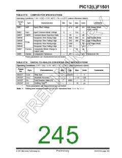
TABLE 27-8: COMPARATOR SPECIFICATIONS
Operating Conditions: 1.8V < VDD < 5.5V, -40°C < TA < +125°C (unless otherwise stated).
Param
Sym.
Characteristics
Min.
Typ.
Max. Units
Comments
No.
CM01
Vioff
Input Offset Voltage
—
±7.5
±60
mV High Power Mode,
Vicm = VDD/2
CM02
Vicm
Input Common Mode Voltage
Common Mode Rejection Ratio
Response Time Rising Edge
Response Time Falling Edge
Response Time Rising Edge
Response Time Falling Edge
0
—
50
VDD
—
V
CM03*
CM04A
CM04B
CM04C
CM04D
CM05*
CMRR
—
—
—
—
—
—
dB
400
200
1200
550
—
800
400
—
ns High Power Mode
ns High Power Mode
Tresp
ns Low Power Mode
—
ns
Tmc2ov Comparator Mode Change to
Output Valid
10
s
CM06
Chyster Comparator Hysteresis
—
65
—
mV Hysteresis ON
*
These parameters are characterized but not tested.
TABLE 27-9: DIGITAL-TO-ANALOG CONVERTER (DAC) SPECIFICATIONS
Operating Conditions: 2.5V < VDD < 5.5V, -40°C < TA < +125°C (unless otherwise stated).
Param
No.
Sym.
Characteristics
Step Size
Min.
Typ.
Max.
Units
Comments
DAC01*
DAC02*
DAC03*
DAC04*
*
CLSB
—
—
—
—
VDD/32
—
—
1/2
—
V
LSb
CACC
CR
Absolute Accuracy
Unit Resistor Value (R)
Settling Time(1)
5000
—
CST
10
s
These parameters are characterized but not tested.
Note 1: Settling time measured while DACR<4:0> transitions from ‘0000’ to ‘1111’.
2011 Microchip Technology Inc.
Preliminary
DS41615A-page 245

 MICROCHIP [ MICROCHIP ]