MCP7940M
2.0
PIN DESCRIPTIONS
The descriptions of the pins are listed in Table 2-1.
TABLE 2-1:
Pin Name
PIN DESCRIPTIONS
Pin Function
VSS
SDA
SCL
X1
Ground
Bidirectional Serial Data
Serial Clock
Xtal Input, External Oscillator Input
Xtal Output
X2
NC
Not Connected
MFP
VCC
Multi-Function Pin
+1.8V to +5.5V Power Supply
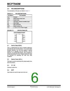
FIGURE 2-1:
DEVICE PINOUTS
SOIC/DFN/MSOP/TSSOP
X1
1
8
VCC
X2
2
3
7
6
MFP
SCL
NC
VSS
4
5
SDA
2.1
Serial Data (SDA)
This is a bidirectional pin used to transfer addresses
and data into and out of the device. It is an open-drain
terminal, therefore, the SDA bus requires a pull-up
resistor to VCC (typically 10 k for 100 kHz, 2 kfor
400 kHz). For normal data transfer, SDA is allowed to
change only during SCL low. Changes during SCL high
are reserved for indicating the Start and Stop
conditions.
2.2
Serial Clock (SCL)
This input is used to synchronize the data transfer from
and to the device.
2.3
X1, X2
External Crystal Pins.
2.4
MFP
Open-drain pin used for alarm and clock-out.
DS22292A-page 6
Preliminary
2012 Microchip Technology Inc.

 MICROCHIP [ MICROCHIP ]