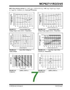
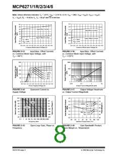
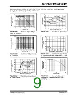
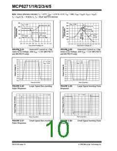
MCP6271/1R/2/3/4/5
2.0
TYPICAL PERFORMANCE CURVES
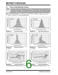
Note:
The graphs and tables provided following this note are a statistical summary based on a limited number of
samples and are provided for informational purposes only. The performance characteristics listed herein
are not tested or guaranteed. In some graphs or tables, the data presented may be outside the specified
operating range (e.g., outside specified power supply range) and therefore outside the warranted range.
Note: Unless otherwise indicated, TA = +25°C, VDD = +2.0V to +5.5V, VSS = GND, VCM = VDD/2, VOUT ≈ VDD/2,
VL = VDD/2, RL = 10 kΩ to VL, CL = 60 pF and CS is tied low.
18%
16%
14%
12%
10%
8%
14%
12%
10%
8%
832 Samples
CM = VSS
832 Samples
VCM = VSS
TA = -40°C to +125°C
V
6%
6%
4%
4%
2%
2%
0%
0%
Input Offset Voltage (mV)
Input Offset Voltage Drift (µV/°C)
FIGURE 2-1:
Input Offset Voltage.
FIGURE 2-4:
Input Offset Voltage Drift.
32%
22%
422 Samples
TA = +125°C
422 Samples
A = 85°C
20%
18%
16%
14%
12%
10%
8%
28%
24%
20%
16%
12%
8%
T
6%
4%
4%
2%
0%
0%
0
10 20 30 40 50 60 70 80 90 100
Input Bias Current (pA)
Input Bias Current (nA)
FIGURE 2-2:
Input Bias Current at
FIGURE 2-5:
Input Bias Current at
T = +85°C.
T = +125°C.
A
A
300
300
VDD = 2.0V
VDD = 5.5V
250
200
150
100
50
250
200
150
100
50
TA = +125°C
TA = +85°C
TA = +125°C
TA
TA
TA
=
=
=
+85°C
+25°C
-40°C
0
0
T
T
A = +25°C
A = -40°C
-50
-100
-50
-100
Common Mode Input Voltage (V)
Common Mode Input Voltage (V)
FIGURE 2-3:
Input Offset Voltage vs.
FIGURE 2-6:
Input Offset Voltage vs.
Common Mode Input Voltage, with V = 2.0V.
Common Mode Input Voltage, with V = 5.5V.
DD
DD
DS21810F-page 6
© 2008 Microchip Technology Inc.

 MICROCHIP [ MICROCHIP ]