MCP6271/1R/2/3/4/5
DC ELECTRICAL SPECIFICATIONS (CONTINUED)
Electrical Characteristics: Unless otherwise indicated, TA = +25°C, VDD = +2.0V to +5.5V, VSS = GND, VCM = VDD/2,
VOUT ≈ VDD/2, VL = VDD/2, RL = 10 kΩ to VL and CS is tied low. (Refer to Figure 1-2 and Figure 1-3).
Parameters
Sym
Min
Typ
Max
Units
Conditions
Output
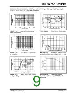
Maximum Output Voltage Swing
Output Short Circuit Current
Power Supply
VOL, VOH VSS + 15
—
VDD − 15
mV 0.5V input overdrive (Note 4)
ISC
—
±25
—
mA
Supply Voltage
VDD
IQ
2.0
—
6.0
V
Quiescent Current per Amplifier
100
170
240
µA
IO = 0
Note 1: The MCP6275’s VCM for op amp B (pins VOUTA/VINB+ and VINB–) is VSS + 100 mV.
2: The current at the MCP6275’s VINB– pin is specified by IB only.
3: This specification does not apply to the MCP6275’s VOUTA/VINB+ pin.
4: The MCP6275’s VINB– pin (op amp B) has a common mode input voltage range (VCMR) of VSS + 100 mV to
DD – 100 mV. CMRR is not measured for op amp B of the MCP6275. The MCP6275’s VOUTA/VINB+ pin (op amp B)
V
has a voltage range specified by VOH and VOL
5: Set by design and characterization.
.
6: Does not apply to op amp B of the MCP6275.
7: All parts with date codes November 2007 and later have been screened to ensure operation at VDD = 6.0V. However,
the other minimum and maximum specifications are measured at 2.0V and 5.5V.
AC ELECTRICAL SPECIFICATIONS
Electrical Characteristics: Unless otherwise indicated, TA = +25°C, VDD = +2.0V to +5.5V, VSS = GND, VCM = VDD/2,
VOUT ≈ VDD/2, VL = VDD/2, RL = 10 kΩ to VL, CL = 60 pF and CS is tied low. (Refer to Figure 1-2 and Figure 1-3).
Parameters
Sym
Min
Typ
Max
Units
Conditions
AC Response
Gain Bandwidth Product
Phase Margin
GBWP
PM
—
—
—
2.0
65
—
—
—
MHz
°
G = +1 V/V
Slew Rate
SR
0.9
V/µs
Noise
Input Noise Voltage
Input Noise Voltage Density
Input Noise Current Density
Eni
eni
ini
—
—
—
4.6
20
3
—
—
—
µVP-P f = 0.1 Hz to 10 Hz
nV/√Hz f = 1 kHz
fA/√Hz f = 1 kHz
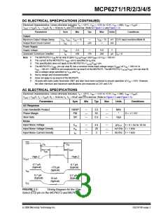
CS
VIL
VIH
tOFF
tON
High-Z
High-Z
VOUT
-0.7 µA
(typical)
-0.7 µA
(typical)
-170 µA
(typical)
ISS
0.7 µA
(typical)
0.7 µA
(typical)
10 nA
(typical)
ICS
FIGURE 1-1:
Timing Diagram for the Chip
Select (CS) pin on the MCP6273 and MCP6275.
© 2008 Microchip Technology Inc.
DS21810F-page 3

 MICROCHIP [ MICROCHIP ]