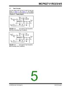
MCP6271/1R/2/3/4/5
† Notice: Stresses above those listed under “Absolute
Maximum Ratings” may cause permanent damage to the
device. This is a stress rating only and functional operation of
the device at those or any other conditions above those
indicated in the operational listings of this specification is not
implied. Exposure to maximum rating conditions for extended
periods may affect device reliability.
1.0
ELECTRICAL
CHARACTERISTICS
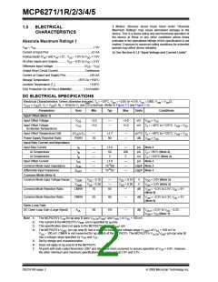
Absolute Maximum Ratings †
VDD – VSS ........................................................................7.0V
Current at Input Pins ....................................................±2 mA
Analog Inputs (VIN+ and VIN–) †† .. VSS – 1.0V to VDD + 1.0V
All other Inputs and Outputs .......... VSS – 0.3V to VDD + 0.3V
†† See Section 4.1.2 “Input Voltage and Current Limits”.
Difference Input Voltage ...................................... |VDD – VSS
|
Output Short Circuit Current .................................Continuous
Current at Output and Supply Pins ............................±30 mA
Storage Temperature....................................–65°C to +150°C
Junction Temperature (TJ) ..........................................+150°C
ESD Protection On All Pins (HBM/MM) ................ ≥ 4 kV/400V
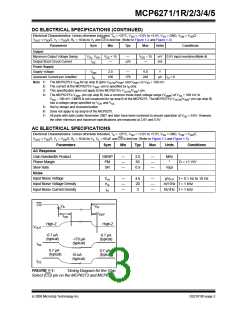
DC ELECTRICAL SPECIFICATIONS
Electrical Characteristics: Unless otherwise indicated, TA = +25°C, VDD = +2.0V to +5.5V, VSS = GND, VCM = VDD/2,
VOUT ≈ VDD/2, VL = VDD/2, RL = 10 kΩ to VL and CS is tied low. (Refer to Figure 1-2 and Figure 1-3).
Parameters
Sym
Min
Typ
Max
Units
Conditions
Input Offset (Note 1)
Input Offset Voltage
VOS
VOS
–3.0
–5.0
—
—
+3.0
+5.0
mV VCM = VSS
Input Offset Voltage
mV TA = –40°C to +125°C, VCM = VSS
(Extended Temperature)
Input Offset Temperature Drift
Power Supply Rejection Ratio
Input Bias Current and Impedance
Input Bias Current
ΔVOS/ΔTA
—
±1.7
90
—
—
µV/°C TA = –40°C to +125°C, VCM = VSS
PSRR
70
dB
VCM = VSS
IB
IB
—
—
—
—
—
—
±1.0
50
—
200
5
pA
pA
nA
pA
Note 2
At Temperature
TA= +85°C (Note 2)
TA= +125°C (Note 2)
Note 3
At Temperature
IB
2
Input Offset Current
IOS
ZCM
ZDIFF
±1.0
1013||6
1013||3
—
—
—
Common Mode Input Impedance
Differential Input Impedance
Common Mode (Note 4)
Common Mode Input Voltage Range
Ω||pF Note 3
Ω||pF Note 3
VCMR
VCMR
VSS − 0.15
VSS − 0.30
70
—
—
85
VDD + 0.15
VDD + 0.30
—
V
V
VDD = 2.0V (Note 5)
VDD = 5.5V (Note 5)
Common Mode Rejection Ratio
Common Mode Rejection Ratio
CMRR
dB
VCM = –0.3V to 2.5V, VDD = 5V
(Note 6)
CMRR
AOL
65
90
80
—
—
dB
dB
VCM = –0.3V to 5.3V, VDD = 5V
(Note 6)
Open-Loop Gain
DC Open-Loop Gain (Large Signal)
110
VOUT = 0.2V to VDD – 0.2V,
V
CM = VSS (Note 1)
Note 1: The MCP6275’s VCM for op amp B (pins VOUTA/VINB+ and VINB–) is VSS + 100 mV.
2: The current at the MCP6275’s VINB– pin is specified by IB only.
3: This specification does not apply to the MCP6275’s VOUTA/VINB+ pin.
4: The MCP6275’s VINB– pin (op amp B) has a common mode input voltage range (VCMR) of VSS + 100 mV to
DD – 100 mV. CMRR is not measured for op amp B of the MCP6275. The MCP6275’s VOUTA/VINB+ pin (op amp B)
V
has a voltage range specified by VOH and VOL
5: Set by design and characterization.
.
6: Does not apply to op amp B of the MCP6275.
7: All parts with date codes November 2007 and later have been screened to ensure operation at VDD = 6.0V. However,
the other minimum and maximum specifications are measured at 2.0V and 5.5V.
DS21810F-page 2
© 2008 Microchip Technology Inc.

 MICROCHIP [ MICROCHIP ]