MCP6271/1R/2/3/4/5
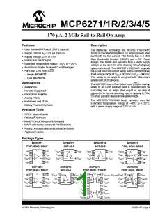
TEMPERATURE SPECIFICATIONS
Electrical Characteristics: Unless otherwise indicated, VDD = +2.0V to +5.5V and VSS = GND.
Parameters
Temperature Ranges
Sym
Min
Typ
Max
Units
Conditions
Specified Temperature Range
Operating Temperature Range
Storage Temperature Range
Thermal Package Resistances
Thermal Resistance, 5L-SOT-23
Thermal Resistance, 6L-SOT-23
Thermal Resistance, 8L-PDIP
Thermal Resistance, 8L-SOIC
Thermal Resistance, 8L-MSOP
Thermal Resistance, 14L-PDIP
Thermal Resistance, 14L-SOIC
Thermal Resistance, 14L-TSSOP
TA
TA
TA
–40
–40
–65
—
—
—
+125
+125
+150
°C
°C
°C
Note
θJA
θJA
θJA
θJA
θJA
θJA
θJA
θJA
—
—
—
—
—
—
—
—
256
230
85
—
—
—
—
—
—
—
—
°C/W
°C/W
°C/W
°C/W
°C/W
°C/W
°C/W
°C/W
163
206
70
120
100
Note:
The Junction Temperature (TJ) must not exceed the Absolute Maximum specification of +150°C.
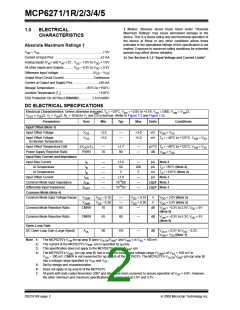
MCP6273/MCP6275 CHIP SELECT SPECIFICATIONS
Electrical Characteristics: Unless otherwise indicated, TA = +25°C, VDD = +2.0V to +5.5V, VSS = GND,
VCM = VDD/2, VOUT ≈ VDD/2, VL = VDD/2, RL = 10 kΩ to VDD/2, CL = 60 pF and CS is tied low.
Parameters
Sym
Min
Typ
Max
Units
Conditions
CS Low Specifications
CS Logic Threshold, Low
CS Input Current, Low
VIL
VSS
—
—
0.2VDD
—
V
ICSL
0.01
µA
CS = VSS
CS High Specifications
CS Logic Threshold, High
CS Input Current, High
VIH
ICSH
ISS
0.8VDD
—
—
VDD
2
V
0.7
µA
µA
µA
CS = VDD
CS = VDD
CS = VDD
GND Current per Amplifier
Amplifier Output Leakage
Dynamic Specifications (Note 1)
—
–0.7
0.01
—
—
—
—
CS Low to Valid Amplifier
Output, Turn on Time
tON
—
4
10
µs
CS Low ≤ 0.2 VDD, G = +1 V/V,
VIN = VDD/2, VOUT = 0.9 VDD/2,
VDD = 5.0V
CS High to Amplifier Output
High-Z
tOFF
—
—
0.01
0.6
—
—
µs
V
CS High ≥ 0.8 VDD, G = +1 V/V,
VIN = VDD/2, VOUT = 0.1 VDD/2
Hysteresis
VHYST
VDD = 5V
Note 1: The input condition (VIN) specified applies to both op amp A and B of the MCP6275. The dynamic
specification is tested at the output of op amp B (VOUTB).
DS21810F-page 4
© 2008 Microchip Technology Inc.

 MICROCHIP [ MICROCHIP ]