MCP6271/1R/2/3/4/5
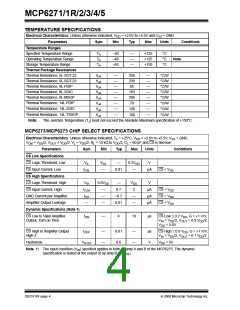
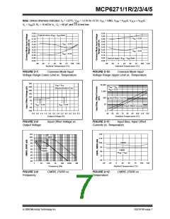
Note: Unless otherwise indicated, TA = +25°C, VDD = +2.0V to +5.5V, VSS = GND, VCM = VDD/2, VOUT ≈ VDD/2,
VL = VDD/2, RL = 10 kΩ to VL, CL = 60 pF and CS is tied low.
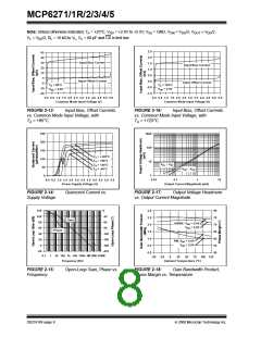
2.5
55
2.0
1.5
45
35
25
15
5
Input Bias Current
Input Offset Current
Input Bias Current
Input Offset Current
1.0
0.5
0.0
-5
TA = 125°C
DD = 5.5V
TA = 85°C
DD = 5.5V
-0.5
-1.0
-15
-25
V
V
0.0 0.5 1.0 1.5 2.0 2.5 3.0 3.5 4.0 4.5 5.0 5.5
Common Mode Input Voltage (V)
0.0 0.5 1.0 1.5 2.0 2.5 3.0 3.5 4.0 4.5 5.0 5.5
Common Mode Input Voltage (V)
FIGURE 2-13:
Input Bias, Offset Currents
FIGURE 2-16:
Input Bias, Offset Currents
vs. Common Mode Input Voltage, with
vs. Common Mode Input Voltage, with
T = +85°C.
T = +125°C.
A
A
250
200
150
100
50
1000
100
10
TA = +125°C
A = +85°C
TA = +25°C
A = -40°C
T
VOL – VSS
T
VDD – VOH
1
0
0.01
0.1
1
10
0.0 0.5 1.0 1.5 2.0 2.5 3.0 3.5 4.0 4.5 5.0 5.5
Power Supply Voltage (V)
Output Current Magnitude (mA)
FIGURE 2-14:
Quiescent Current vs.
FIGURE 2-17:
Output Voltage Headroom
Supply Voltage.
vs. Output Current Magnitude.
120
100
80
0
3.0
2.5
80
75
70
65
60
55
50
-30
Gain
-60
GBWP, VDD = 5.5V
VDD = 2.0V
2.0
1.5
1.0
0.5
0.0
60
-90
Phase
40
20
0
-120
-150
-180
-210
PM, VDD = 5.5V
VDD = 2.0V
-20
0.1
1
10 100 1k 10k 100k 1M10M 100M
-50 -25
0
25
50
75 100 125
Frequency (Hz)
Ambient Temperature (°C)
FIGURE 2-15:
Open-Loop Gain, Phase vs.
FIGURE 2-18:
Gain Bandwidth Product,
Frequency.
Phase Margin vs. Temperature.
DS21810F-page 8
© 2008 Microchip Technology Inc.

 MICROCHIP [ MICROCHIP ]