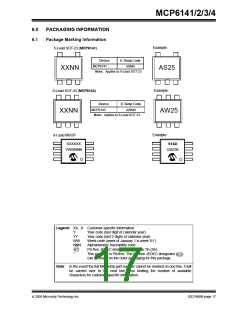
MCP6141/2/3/4
EQUATION 4-2:
GN = 1 +
4.4.2
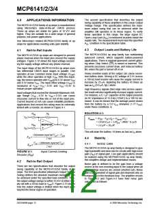
CAPACITIVE LOADS
Driving large capacitive loads can cause stability
problems for voltage feedback op amps. As the load
capacitance increases, the feedback loop’s phase
margin decreases and the closed-loop bandwidth is
reduced. This produces gain peaking in the frequency
response, with overshoot and ringing in the step
response. A unity gain buffer (G = +1) is the most
sensitive to capacitive loads, though all gains show the
same general behavior.
RF
------
RG
≥ 10 V/V
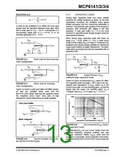
In order for the amplifiers to be stable, the noise gain
should meet the specified minimum noise gain. Note
that a noise gain of GN = +10 V/V corresponds to a
non-inverting signal gain of G = +10 V/V, or to an
inverting signal gain of G = -9 V/V.
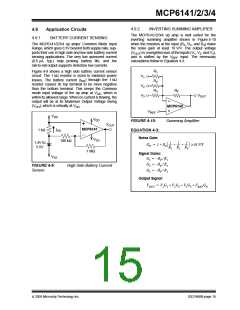
When driving large capacitive loads with these op
amps (e.g., > 60 pF when G = +10), a small series
resistor at the output (RISO in Figure 4-5) improves the
feedback loop’s phase margin (stability) by making the
output load resistive at higher frequencies. The band-
width will be generally lower than the bandwidth with no
capacitive load.
RIN
VIN
VOUT
MCP614X
RG
RF
RG
RF
VA
FIGURE 4-2:
Noise Gain for Non-inverting
Gain Configuration.
RISO
CL
VOUT
MCP614X
RG
RF
VB
VIN
VOUT
FIGURE 4-5:
Output Resistor, RISO
MCP614X
RIN
stabilizes large capacitive loads.
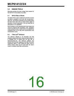
Figure 4-6 gives recommended RISO values for differ-
ent capacitive loads and gains. The x-axis is the nor-
malized load capacitance (CL/GN), where GN is the
circuit’s noise gain. For non-inverting gains, GN and the
Signal Gain are equal. For inverting gains, GN is
1+|Signal Gain| (e.g., -9 V/V gives GN = +10 V/V).
FIGURE 4-3:
Gain Configuration.
Noise Gain for Inverting
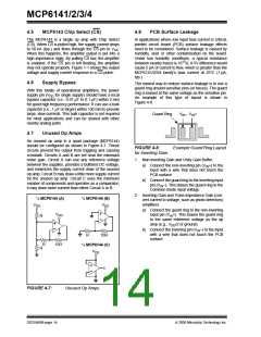
Figure 4-4 shows a unity gain buffer and Miller integra-
tor that are unstable when used with the
MCP6141/2/3/4 family. Note that the capacitor makes
the integrator circuit reach unity gain at high
frequencies, which makes these op amps unstable.
1001,000k
Unity Gain Buffer
10k
10,0 0
GN = +10
GN = +20
GN t+50
VOUT
MCP614X
VIN
1k
1,000
1p
10p
1.E+01
Normalized Load Capacitance; CL/GN (F)
100p
1n
1.E+03
1.E+00
1.E+02
Miller Integrator
R
C
FIGURE 4-6:
Recommended RISO Values
VOUT
VIN
for Capacitive Loads.
MCP614X
After selecting RISO for your circuit, double check the
resulting frequency response peaking and step
response overshoot. Modify RISO’s value until the
response is reasonable. Bench evaluation and simula-
tions with the MCP6141/2/3/4 SPICE macro model are
helpful.
FIGURE 4-4:
Typical Unstable Circuits for
the MCP6141/2/3/4 Family.
© 2005 Microchip Technology Inc.
DS21668B-page 13

 MICROCHIP [ MICROCHIP ]