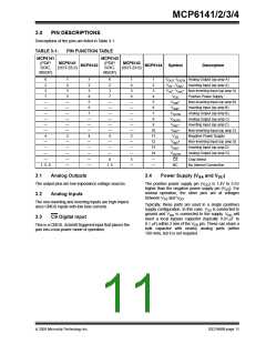
MCP6141/2/3/4
4.9.2
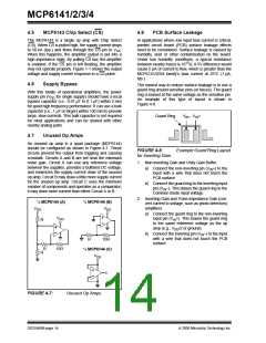
INVERTING SUMMING AMPLIFIER
4.9
Application Circuits
The MCP6141/2/3/4 op amp is well suited for the
inverting summing amplifier shown in Figure 4-10
when the resistors at the input (R1, R2, and R3) make
the noise gain at least 10 V/V. The output voltage
(VOUT) is a weighted sum of the inputs (V1, V2, and V3),
and is shifted by the VREF input. The necessary
calculations follow in Equation 4-3.
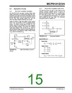
4.9.1
BATTERY CURRENT SENSING
The MCP6141/2/3/4 op amps’ Common Mode Input
Range, which goes 0.3V beyond both supply rails, sup-
ports their use in high side and low side battery current
sensing applications. The very low quiescent current
(0.6 μA, typ.) help prolong battery life, and the
rail-to-rail output supports detection low currents.
.
Figure 4-9 shows a high side battery current sensor
circuit. The 1 kΩ resistor is sized to minimize power
losses. The battery current (IDD) through the 1 kΩ
resistor causes its top terminal to be more negative
than the bottom terminal. This keeps the Common
mode input voltage of the op amp at VDD, which is
within its allowed range. When no current is flowing, the
output will be at its Maximum Output Voltage Swing
R1
V1
R2
V2
R3
RF
VOUT
V3
(VOH), which is virtually at VDD
.
MCP614X
.
VREF
VDD
VDD
MCP6141
VSS
FIGURE 4-10:
Summing Amplifier.
VOUT
IDD
100 kΩ
1 kΩ
EQUATION 4-3:
Noise Gain:
1.4V to
5.5V
1
1
1
⎞
⎛
GN = 1 + RF ----- + ----- + ----- ≥ 10 V/V
⎝
⎠
R1 R2 R3
1 MΩ
Signal Gains:
G1 = –RF ⁄ R1
VSS
G2 = –RF ⁄ R2
G3 = –RF ⁄ R3
FIGURE 4-9:
Sensor.
High Side Battery Current
Output Signal:
VOUT = V1G1 + V2G2 + V3G3 + VREFGN
© 2005 Microchip Technology Inc.
DS21668B-page 15

 MICROCHIP [ MICROCHIP ]