MCP6141/2/3/4
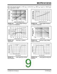
The second specification that describes the output
swing capability of these amplifiers is the Linear Output
Voltage Range. This specification defines the maxi-
mum output swing that can be achieved while the
amplifier still operates in its linear region. To verify
linear operation in this range, the large signal DC
Open-Loop Gain (AOL) is measured at points inside the
supply rails. The measurement must meet the specified
4.0
APPLICATIONS INFORMATION
The MCP6141/2/3/4 family of op amps is manufactured
using Microchip’s state-of-the-art CMOS process
These op amps are stable for gains of 10 V/V and
higher. They are suitable for a wide range of general
purpose, low-power applications.
See Microchip’s related MCP6041/2/3/4 family of op
amps for applications needing unity gain stability.
AOL condition in the specification table.
4.3
Output Loads and Battery Life
4.1
Rail-to-Rail Inputs
The MCP6141/2/3/4 op amp family has outstanding
quiescent current, which supports battery-powered
applications. There is minimal quiescent current glitch-
ing when Chip Select (CS) is raised or lowered. This
prevents excessive current draw, and reduced battery
life, when the part is turned off or on.
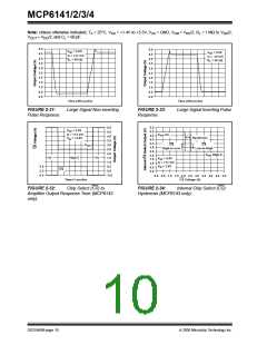
The MCP6141/2/3/4 op amps are designed to prevent
phase reversal when the input pins exceed the supply
voltages. Figure 2-10 shows the input voltage exceed-
ing the supply voltage without any phase reversal.
The input stage of the MCP6141/2/3/4 op amps uses
two differential CMOS input stages in parallel. One
operates at low Common mode input voltage (VCM),
while the other operates at high VCM. With this topol-
ogy, the device operates with VCM tp to 0.3V above VDD
and 0.3V below VSS. The input offset voltage (VOS) is
measured at VCM = VSS – 0.3V and VDD + 0.3V to
ensure proper operation.
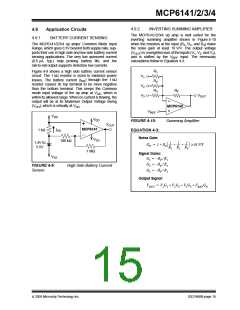
Heavy resistive loads at the output can cause exces-
sive battery drain. Driving a DC voltage of 2.5V across
a 100 kΩ load resistor will cause the supply current to
increase by 25 μA, depleting the battery 43 times as
fast as IQ (0.6 μA, typ.) alone.
High frequency signals (fast edge rate) across capaci-
tive loads will also significantly increase supply current.
For instance, a 0.1 μF capacitor at the output presents
an AC impedance of 15.9 kΩ (1/2πfC) to a 100 Hz sin-
ewave. It can be shown that the average power drawn
from the battery by a 5.0 Vp-p sinewave (1.77 Vrms),
under these conditions, is
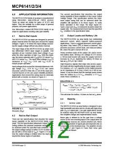
Input voltages that exceed the Absolute Maximum Volt-
age Range (VSS – 0.3V to VDD + 0.3V) can cause
excessive current to flow into or out of the input pins.
Current beyond ±2 mA can cause reliability problems.
Applications that exceed this rating must be externally
limited with a resistor, as shown in Figure 4-1.
EQUATION 4-1:
RIN
RF
VA
VB
PSupply = (VDD - VSS) (IQ + VL(p-p) f CL )
= (5V)(0.6 µA + 5.0Vp-p · 100Hz · 0.1µF)
= 3.0 µW + 50 µW
VOUT
MCP614X
RIN
This will drain the battery 18 times as fast as IQ alone.
(Maximum expected VIN) – VDD
------------------------------------------------------------------------------
2 mA
RIN
≥
4.4
Stability
NOISE GAIN
VSS – (Minimum expected VIN
)
4.4.1
---------------------------------------------------------------------------
2 mA
RIN
≥
The MCP6141/2/3/4 op amp family is designed to give
high bandwidth and slew rate for circuits with high noise
gain (GN) or signal gain. Low gain applications should
be realized using the MCP6041/2/3/4 op amp family;
this simplifies design and implementation issues.
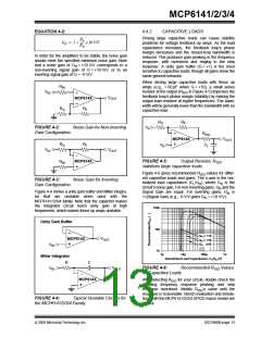
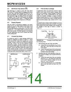
FIGURE 4-1:
Resistor (RIN).
Input Current-Limiting
4.2
Rail-to-Rail Output
Noise gain is defined to be the gain from a voltage
source at the non-inverting input to the output when all
other voltage sources are zeroed (shorted out). Noise
gain is independent of signal gain and depends only on
components in the feedback loop. The amplifier circuits
in Figure 4-2 and Figure 4-3 have their noise gain
calculated as follows:
There are two specifications that describe the output
swing capability of the MCP6141/2/3/4 family of op
amps. The first specification (Maximum Output Voltage
Swing) defines the absolute maximum swing that can
be achieved under the specified load condition. Thus,
the output voltage swings to within 10 mV of either sup-
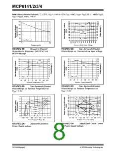
ply rail with a 50 kΩ load to VDD/2. Figure 2-10 shows
how the output voltage is limited when the input goes
beyond the linear region of operation.
DS21668B-page 12
© 2005 Microchip Technology Inc.

 MICROCHIP [ MICROCHIP ]