MCP6141/2/3/4
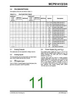
3.0
PIN DESCRIPTIONS
Descriptions of the pins are listed in Table 3-1.
TABLE 3-1:
PIN FUNCTION TABLE
MCP6143
MCP6141
(PDIP,
MCP6141
(PDIP,
SOIC,
MCP6143
(SOT-23-6)
MCP6142
MCP6144
Symbol
Description
SOIC,
(SOT-23-5)
MSOP)
MSOP)
6
2
1
4
1
2
6
1
4
1
2
V
, V
Analog Output (op amp A)
Inverting Input (op amp A)
Non-inverting Input (op amp A)
Positive Power Supply
OUT OUTA
2
V
–, V
+, V
–
+
IN
INA
3
3
3
3
3
3
V
IN
INA
7
5
8
7
6
4
V
DD
—
—
—
—
—
—
4
—
—
—
—
—
—
2
5
—
—
—
—
—
—
4
—
—
—
—
—
—
2
5
V
+
Non-inverting Input (op amp B)
Inverting Input (op amp B)
Analog Output (op amp B)
Analog Output (op amp C)
Inverting Input (op amp C)
Non-inverting Input (op amp C)
Negative Power Supply
INB
INB
6
6
V
–
7
7
V
V
OUTB
OUTC
—
—
—
4
8
9
V
V
–
+
INC
INC
10
11
12
13
14
V
SS
—
—
—
—
—
—
—
—
—
—
—
—
—
—
—
V
V
+
Non-inverting Input (op amp D)
Inverting Input (op amp D)
Analog Output (op amp D)
IND
IND
–
V
OUTD
CS
—
—
—
—
—
8
5
—
—
Chip Select
1, 5, 8
1, 5
—
NC
No Internal Connection
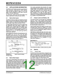
3.1
Analog Outputs
3.4
Power Supply (V and V
)
DD
SS
The output pins are low-impedance voltage sources.
The positive power supply pin (VDD) is 1.4V to 5.5V
higher than the negative power supply pin (VSS). For
normal operation, the other pins are at voltages
3.2
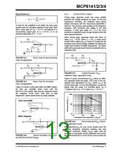
Analog Inputs
between VSS and VDD
.
The non-inverting and inverting inputs are high-imped-
ance CMOS inputs with low bias currents.
Typically, these parts are used in a single (positive)
supply configuration. In this case, VSS is connected to
ground and VDD is connected to the supply. VDD will
need a local bypass capacitor (typically 0.01 μF to
0.1 μF) within 2 mm of the VDD pin. These can share a
bulk capacitor with nearby analog parts (within
100 mm), but it is not required.
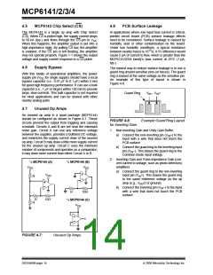
3.3
CS Digital Input
This is a CMOS, Schmitt-triggered input that places the
part into a low-power mode of operation.
© 2005 Microchip Technology Inc.
DS21668B-page 11

 MICROCHIP [ MICROCHIP ]