MCP6141/2/3/4
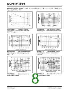
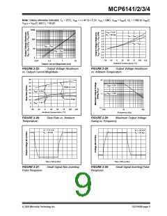
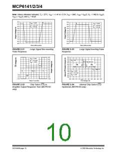
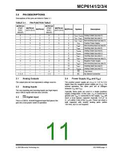
Note: Unless otherwise indicated, TA = 25°C, VDD = +1.4V to +5.5V, VSS = GND, VCM = VDD/2, RL = 1 MΩ to VDD/2,
VOUT ≈ VDD/2, and CL = 60 pF.
1000
5.0
VDD = 5.5V
4.5
RL = 50 kΩ
4.0
3.5
3.0
2.5
2.0
1.5
1.0
0.5
0.0
VOL – VSS
100
10
1
VDD – VOH
VDD – VOH
VOL – VSS
-50
-25
0
25
50
75
100 125
0.01
0.1
1
10
Ambient Temperature (°C)
Output Current Magnitude (mA)
FIGURE 2-25:
Output Voltage Headroom
FIGURE 2-28:
Output Voltage Headroom
vs. Output Current Magnitude.
vs. Ambient Temperature.
40
35
30
10
VDD = 5.5V
High-to-Low
Low-to-High
25
VDD = 5.5V
20
VDD = 1.4V
1
15
10
VDD = 1.4V
-25
5
0
0.1
-50
0
25
50
75
100
125
100
1k
10k
1.E+04
1.E+02
1.E+03
Ambient Temperature (°C)
Frequency (Hz)
FIGURE 2-26:
Slew Rate vs. Ambient
FIGURE 2-29:
Maximum Output Voltage
Temperature.
Swing vs. Frequency.
80
60
80
60
G = +11 V/V
RL = 50 kΩ
G = -10 V/V
RL = 50 kΩ
40
40
20
20
0
0
-20
-40
-60
-80
-20
-40
-60
-80
0.0 0.1 0.2 0.3 0.4 0.5 0.6 0.7 0.8 0.9 1.0
Time (100 µs/div)
0.0 0.1 0.2 0.3 Ti0m.4e (100.05µs0/d.6iv) 0.7 0.8 0.9 1.0
FIGURE 2-27:
Pulse Response.
Small Signal Non-inverting
FIGURE 2-30:
Response.
Small Signal Inverting Pulse
© 2005 Microchip Technology Inc.
DS21668B-page 9

 MICROCHIP [ MICROCHIP ]