MCP414X/416X/424X/426X
STATUS register can be accessed via the READ
commands. Register 4-1 describes each STATUS
register bit.
4.2.2.1
Status (STATUS) Register
This register contains 5 status bits. These bits show the
state of the WiperLock bits, the Shutdown bit the Write
Protect bit, and if an EEPROM write cycle is active. The
The STATUS register is placed at Address 05h.
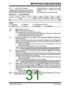
REGISTER 4-1:
STATUS REGISTER
R-1 R-1
R-1
R-1
R-0
R-x
R-x
R-x
R-x
(1)
(1)
D8:D5
EEWA
WL1
WL0
SHDN
WP (1)
bit 7
bit 0
Legend:
R = Readable bit
W = Writable bit
‘1’ = Bit is set
U = Unimplemented bit, read as ‘0’
‘0’ = Bit is cleared x = Bit is unknown
-n = Value at POR
bit 8-5
bit 4
D8:D5: Reserved. Forced to “1”
EEWA: EEPROM Write Active Status bit
This bit indicates if the EEPROM Write Cycle is occurring.
1= An EEPROM Write cycle is currently occurring. Only serial commands to the Volatile memory
locations are allowed (addresses 00h, 01h, 04h, and 05h)
0= An EEPROM Write cycle is NOT currently occurring
bit 3
bit 2
bit 1
WL1: WiperLock Status bit for Resistor Network 1 (Refer to Section 5.3 “WiperLock™ Technology”
for further information)
WiperLock (WL) prevents the Volatile and Non-Volatile Wiper 1 addresses and the TCON register bits
R1HW, R1A, R1W, and R1B from being written to. High Voltage commands are required to enable and
disable WiperLock Technology.
1= Wiper and TCON register bits R1HW, R1A, R1W, and R1B of Resistor Network 1 (Pot 1) are
“Locked” (Write Protected)
0= Wiper and TCON of Resistor Network 1 (Pot 1) can be modified
Note:
The WL1 bit always reflects the result of the last programming cycle to the non-volatile WL1
bit. After a POR or BOR event, the WL1 bit is loaded with the non-volatile WL1 bit value.
WL0: WiperLock Status bit for Resistor Network 0 (Refer to Section 5.3 “WiperLock™ Technology”
for further information)
The WiperLock Technology bits (WLx) prevents the Volatile and Non-Volatile Wiper 0 addresses and the
TCON register bits R0HW, R0A, R0W, and R0B from being written to. High Voltage commands are
required to enable and disable WiperLock Technology.
1= Wiper and TCON register bits R0HW, R0A, R0W, and R0B of Resistor Network 0 (Pot 0) are
“Locked” (Write Protected)
0= Wiper and TCON of Resistor Network 0 (Pot 0) can be modified
Note:
The WL0 bit always reflects the result of the last programming cycle to the non-volatile WL0
bit. After a POR or BOR event, the WL0 bit is loaded with the non-volatile WL0 bit value.
SHDN: Hardware Shutdown pin Status bit (Refer to Section 5.4 “Shutdown” for further information)
This bit indicates if the Hardware shutdown pin (SHDN) is low. A hardware shutdown disconnects the
Terminal A and forces the wiper (Terminal W) to Terminal B (see Figure 5-2). While the device is in
Hardware Shutdown (the SHDN pin is low) the serial interface is operational so the STATUS register
may be read.
1= MCP4XXX is in the Hardware Shutdown state
0= MCP4XXX is NOT in the Hardware Shutdown state
Note 1: Requires a High Voltage command to modify the state of this bit (for Non-Volatile devices only). This bit is
Not directly written, but reflects the system state (for this feature).
© 2008 Microchip Technology Inc.
DS22059B-page 31

 MICROCHIP [ MICROCHIP ]