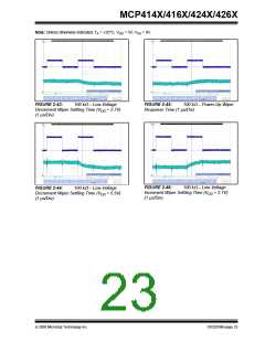
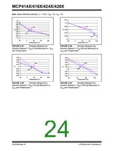
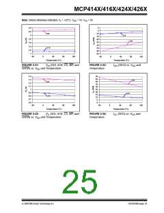
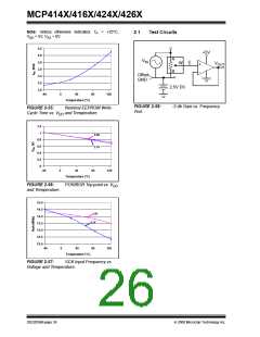
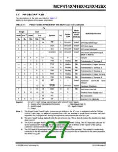
MCP414X/416X/424X/426X
3.0
PIN DESCRIPTIONS
The descriptions of the pins are listed in Table 3-1.
Additional descriptions of the device pins follows.
TABLE 3-1:
PINOUT DESCRIPTION FOR THE MCP414X/416X/424X/426X
Pin
Weak
Pull-up/
down
Single
Dual
Pot
Standard Function
Buffer
Type
Rheo Pot (1) Rheo
Symbol
I/O
(Note 2)
8L
1
8L
1
10L
1
14L
1
16L
16
1
CS
SCK
I
I
I
HV w/ST “smart”
HV w/ST “smart”
HV w/ST “smart”
SPI Chip Select Input
SPI Clock Input
2
2
2
2
3
—
3
3
3
2
SDI
SPI Serial Data Input
—
—
—
—
SDI/SDO
I/O HV w/ST “smart”
SPI Serial Data Input/Output
(Note 1, Note 3)
4
4
—
—
—
5
4
5
4
5
3, 4
5
VSS
P1B
P1W
P1A
P0A
P0W
P0B
WP
—
A
A
A
A
A
A
I
P
—
No
Ground
—
—
—
—
5
Analog
Analog
Analog
Analog
Analog
Analog
I
Potentiometer 1 Terminal B
Potentiometer 1 Wiper Terminal
Potentiometer 1 Terminal A
Potentiometer 0 Terminal A
Potentiometer 0 Wiper Terminal
Potentiometer 0 Terminal B
6
6
6
No
—
—
7
7
7
No
8
8
No
6
9
9
No
6
7
8
10
11
10
12
No
—
—
—
“smart”
Hardware
Protect
EEPROM
Write
—
—
—
8
—
9
12
13
14
—
—
13
14
15
11
17
SHDN
SDO
VDD
NC
I
HV w/ST “smart”
Hardware Shutdown
SPI Serial Data Out
7
O
O
P
No
—
—
—
8
10
—
11
—
—
—
Positive Power Supply Input
No Connection
—
—
9
—
—
9
EP
Exposed Pad. (Note 4)
Legend:
HV w/ST = High Voltage tolerant input (with Schmidtt trigger input)
A = Analog pins (Potentiometer terminals)
O = digital output
I = digital input (high Z)
I/O = Input / Output
P = Power
Note 1: The 8-lead Single Potentiometer devices are pin limited so the SDO pin is multiplexed with the SDI pin
(SDI/SDO pin). After the Address/Command (first 6-bits) are received, If a valid Read command has been
requested, the SDO pin starts driving the requested read data onto the SDI/SDO pin.
2: The pin’s “smart” pull-up shuts off while the pin is forced low. This is done to reduce the standby and shut-
down current.
3: The SDO is an open drain output, which uses the internal “smart” pull-up. The SDI input data rate can be
at the maximum SPI frequency. the SDO output data rate will be limited by the “speed” of the pull-up,
customers can increase the rate with external pull-up resistors.
4: The DFN and QFN packages have a contact on the bottom of the package. This contact is conductively
connected to the die substrate, and therefore should be unconnected or connected to the same ground as
the device’s VSS pin.
© 2008 Microchip Technology Inc.
DS22059B-page 27

 MICROCHIP [ MICROCHIP ]