MCP414X/416X/424X/426X
3.1
Chip Select (CS)
3.7
Potentiometer Terminal A
The CS pin is the serial interface’s chip select input.
Forcing the CS pin to VIL enables the serial commands.
Forcing the CS pin to VIHH enables the high-voltage
serial commands.
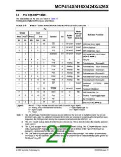
The terminal A pin is available on the MCP4XX1
devices, and is connected to the internal potentiome-
ter’s terminal A.
The potentiometer’s terminal A is the fixed connection
to the Full Scale wiper value of the digital
potentiometer. This corresponds to a wiper value of
0x100 for 8-bit devices or 0x80 for 7-bit devices.
3.2
Serial Data In (SDI)
The SDI pin is the serial interfaces Serial Data In pin.
This pin is connected to the Host Controllers SDO pin.
The terminal A pin does not have a polarity relative to
the terminal W or B pins. The terminal A pin can
support both positive and negative current. The voltage
3.3
Serial Data In / Serial Data Out
(SDI/SDO)
on terminal A must be between VSS and VDD
.
The terminal A pin is not available on the MCP4XX2
devices, and the internally terminal A signal is floating.
On the MCP41X1 devices, pin-out limitations do not
allow for individual SDI and SDO pins. On these
devices, the SDI and SDO pins are multiplexed.
MCP42X1 devices have two terminal A pins, one for
each resistor network.
The MCP41X1 serial interface knows when the pin
needs to change from being an input (SDI) to being an
output (SDO). The Host Controller’s SDO pin must be
properly protected from a drive conflict.
3.8
Write Protect (WP)
The WP pin is used to force the non-volatile memory to
be write protected.
3.4
Ground (VSS)
3.9
Shutdown (SHDN)
The VSS pin is the device ground reference.
The SHDN pin is used to force the resistor network
terminals into the hardware shutdown state.
3.5
Potentiometer Terminal B
The terminal B pin is connected to the internal potenti-
ometer’s terminal B.
3.10 Serial Data Out (SDO)
The SDO pin is the serial interfaces Serial Data Out pin.
This pin is connected to the Host Controllers SDI pin.
The potentiometer’s terminal B is the fixed connection
to the Zero Scale wiper value of the digital potentiome-
ter. This corresponds to a wiper value of 0x00 for both
7-bit and 8-bit devices.
This pin allows the Host Controller to read the digital
potentiometers registers, or monitor the state of the
command error bit.
The terminal B pin does not have a polarity relative to
the terminal W or A pins. The terminal B pin can
support both positive and negative current. The voltage
3.11 Positive Power Supply Input (VDD
)
on terminal B must be between VSS and VDD
.
The VDD pin is the device’s positive power supply input.
The input power supply is relative to VSS
MCP42XX devices have two terminal B pins, one for
each resistor network.
.
While the device VDD < Vmin (2.7V), the electrical
performance of the device may not meet the data sheet
specifications.
3.6
Potentiometer Wiper (W) Terminal
The terminal W pin is connected to the internal potenti-
ometer’s terminal W (the wiper). The wiper terminal is
the adjustable terminal of the digital potentiometer. The
terminal W pin does not have a polarity relative to
terminals A or B pins. The terminal W pin can support
both positive and negative current. The voltage on
3.12 No Connection (NC)
Those pins should be either connected to VDD or VSS
.
3.13 Exposed Pad (EP)
terminal W must be between VSS and VDD
.
This pad is conductively connected to the device's
substrate. This pad should be tied to the same potential
as the VSS pin (or left unconnected). This pad could be
used to assist as a heat sink for the device when
connected to a PCB heat sink.
MCP42XX devices have two terminal W pins, one for
each resistor network.
DS22059B-page 28
© 2008 Microchip Technology Inc.

 MICROCHIP [ MICROCHIP ]