ENC28J60
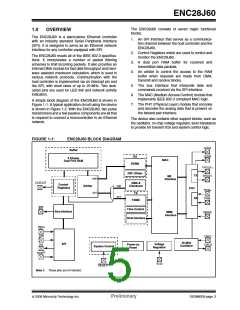
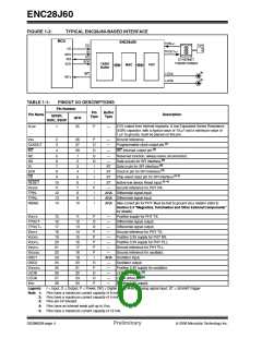
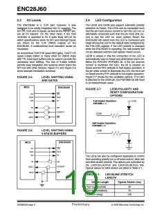
FIGURE 1-2:
TYPICAL ENC28J60-BASED INTERFACE
MCU
ENC28J60
TPIN+/-
RJ45
CS
SI
I/O
TPOUT+/-
SDO
SDI
SO
ETHERNET
TRANSFORMER
SCK
SCK
TX/RX
Buffer
PHY
MAC
INT
LEDA
LEDB
INTX
TABLE 1-1:
PINOUT I/O DESCRIPTIONS
Pin Number
Pin
Type
Buffer
Type
Pin Name
Description
SPDIP,
QFN
SOIC, SSOP
2.5V output from internal regulator. A low Equivalent Series Resistance
(ESR) capacitor, with a typical value of 10 μF and a minimum value of
1 μF to ground, must be placed on this pin.
VCAP
1
25
P
—
VSS
2
3
26
27
28
1
P
O
O
O
O
I
—
—
Ground reference.
(1)
CLKOUT
INT
Programmable clock output pin.
(2)
4
—
INT interrupt output pin.
NC
5
—
Reserved function; always leave unconnected.
(2)
SO
6
2
—
Data out pin for SPI interface.
(3)
SI
7
3
ST
ST
ST
ST
—
Data in pin for SPI interface.
(3)
SCK
CS
8
4
I
Clock in pin for SPI interface.
(3,4)
9
5
I
Chip select input pin for SPI interface.
(3, 4)
RESET
VSSRX
TPIN-
TPIN+
RBIAS
10
11
12
13
14
6
I
Active-low device Reset input.
7
P
I
Ground reference for PHY RX.
8
ANA Differential signal input.
ANA Differential signal input.
9
I
10
I
ANA Bias current pin for PHY. Must be tied to ground via a resistor (refer to
Section 2.4 “Magnetics, Termination and Other External Components”
for details).
VDDTX
TPOUT-
TPOUT+
VSSTX
15
16
17
18
19
20
21
22
23
24
25
26
27
28
11
12
13
14
15
16
17
18
19
20
21
22
23
24
P
O
O
P
P
P
P
P
I
—
—
—
—
—
—
—
—
Positive supply for PHY TX.
Differential signal output.
Differential signal output.
Ground reference for PHY TX.
Positive 3.3V supply for PHY RX.
Positive 3.3V supply for PHY PLL.
Ground reference for PHY PLL.
Ground reference for oscillator.
VDDRX
VDDPLL
VSSPLL
VSSOSC
OSC1
ANA Oscillator input.
OSC2
O
P
O
O
P
—
—
—
—
—
Oscillator output.
VDDOSC
LEDB
Positive 3.3V supply for oscillator.
(5)
LEDB driver pin.
(5)
LEDA
LEDA driver pin.
VDD
Positive 3.3V supply.
Legend:
I = Input, O = Output, P = Power, DIG = Digital input, ANA = Analog signal input, ST = Schmitt Trigger
Note 1: Pins have a maximum current capacity of 8 mA.
2: Pins have a maximum current capacity of 4 mA.
3: Pins are 5V tolerant.
4: Pins have an internal weak pull-up to VDD.
5: Pins have a maximum current capacity of 12 mA.
DS39662B-page 4
Preliminary
© 2006 Microchip Technology Inc.

 MICROCHIP [ MICROCHIP ]