ENC28J60
The ENC28J60 consists of seven major functional
blocks:
1.0
OVERVIEW
The ENC28J60 is a stand-alone Ethernet controller
with an industry standard Serial Peripheral Interface
(SPI). It is designed to serve as an Ethernet network
interface for any controller equipped with SPI.
1. An SPI interface that serves as a communica-
tion channel between the host controller and the
ENC28J60.
2. Control Registers which are used to control and
monitor the ENC28J60.
The ENC28J60 meets all of the IEEE 802.3 specifica-
tions. It incorporates a number of packet filtering
schemes to limit incoming packets. It also provides an
internal DMA module for fast data throughput and hard-
ware assisted checksum calculation, which is used in
various network protocols. Communication with the
host controller is implemented via an interrupt pin and
the SPI, with clock rates of up to 20 MHz. Two dedi-
cated pins are used for LED link and network activity
indication.
3. A dual port RAM buffer for received and
transmitted data packets.
4. An arbiter to control the access to the RAM
buffer when requests are made from DMA,
transmit and receive blocks.
5. The bus interface that interprets data and
commands received via the SPI interface.
6. The MAC (Medium Access Control) module that
implements IEEE 802.3 compliant MAC logic.
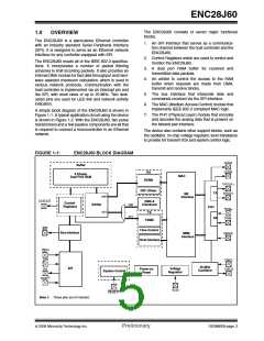
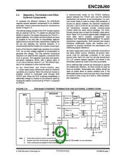
A simple block diagram of the ENC28J60 is shown in
Figure 1-1. A typical application circuit using the device
is shown in Figure 1-2. With the ENC28J60, two pulse
transformers and a few passive components are all that
is required to connect a microcontroller to an Ethernet
network.
7. The PHY (Physical Layer) module that encodes
and decodes the analog data that is present on
the twisted pair interface.
The device also contains other support blocks, such as
the oscillator, on-chip voltage regulator, level translators
to provide 5V tolerant I/Os and system control logic.
FIGURE 1-1:
ENC28J60 BLOCK DIAGRAM
LEDA
Buffer
LEDB
RX
8 Kbytes
Dual Port RAM
MAC
RXBM
TPOUT+
TPOUT-
RXF (Filter)
TX
MII
Interface
ch0
CLKOUT
DMA &
Control
Registers
Arbiter
Checksum
ch0
ch1
PHY
TPIN+
TPIN-
ch1
TX
RX
TXBM
INT
Flow Control
Host Interface
Bus Interface
MIIM
Interface
RBIAS
CS(1)
SI(1)
OSC1
OSC2
25 MHz
Oscillator
SPI
Voltage
Regulator
Power-on
Reset
SO
System Control
SCK(1)
VCAP
RESET(1)
Note 1: These pins are 5V tolerant.
© 2006 Microchip Technology Inc.
Preliminary
DS39662B-page 3

 MICROCHIP [ MICROCHIP ]