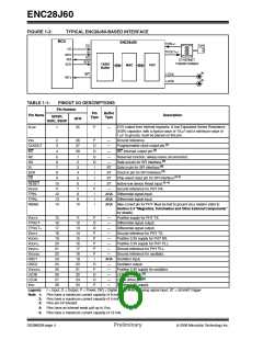
ENC28J60
2.5
I/O Levels
2.6
LED Configuration
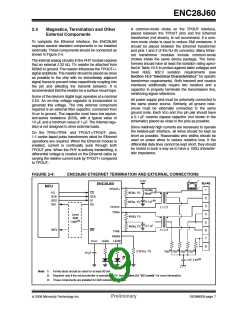
The ENC28J60 is a 3.3V part; however, it was
designed to be easily integrated into 5V systems. The
SPI CS, SCK and SI inputs, as well as the RESET pin,
are all 5V tolerant. On the other hand, if the host
controller is operated at 5V, it quite likely will not be
within specifications when its SPI and interrupt inputs
are driven by the 3.3V CMOS outputs on the
ENC28J60. A unidirectional level translator would be
necessary.
The LEDA and LEDB pins support automatic polarity
detection on Reset. The LEDs can be connected such
that the pin must source current to turn the LED on, or
alternately connected such that the pin must sink cur-
rent to turn the LED on. Upon system Reset, the
ENC28J60 will detect how the LED is connected and
begin driving the LED to the default state configured by
the PHLCON register. If the LED polarity is changed
while the ENC28J60 is operating, the new polarity will
not be detected until the next system Reset occurs.
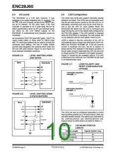
An economical 74HCT08 (quad AND gate), 74ACT125
(quad 3-state buffer) or many other 5V CMOS chips
with TTL level input buffers may be used to provide the
necessary level shifting. The use of 3-state buffers
permits easy integration into systems which share the
SPI bus with other devices. Figure 2-5 and Figure 2-6
show example translation schemes.
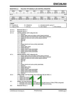
LEDB is unique in that the connection of the LED is
automatically read on Reset and determines how to ini-
tialize the PHCON1.PDPXMD bit. If the pin sources
current to illuminate the LED, the bit is cleared on
Reset and the PHY defaults to half-duplex operation. If
the pin sinks current to illuminate the LED, the bit is set
on Reset and the PHY defaults to full-duplex operation.
Figure 2-7 shows the two available options. If no LED
is attached to the LEDB pin, the PDPXMD bit will reset
to an indeterminate value.
FIGURE 2-5:
MCU
LEVEL SHIFTING USING
AND GATES
ENC28J60
FIGURE 2-7:
LEDB POLARITY AND
RESET CONFIGURATION
OPTIONS
CS
SCK
SI
I/O
SCK
SO
Full-Duplex Operation:
PDPXMD = 1
+3.3V
SO
SI
OSC1
INT0
CLKOUT
LEDB
INT
Half-Duplex Operation:
PDPXMD = 0
FIGURE 2-6:
MCU
LEVEL SHIFTING USING
3-STATE BUFFERS
LEDB
ENC28J60
CS
SCK
SI
I/O
SCK
SO
The LEDs can also be configured separately to control
their operating polarity (on or off when active), blink rate
and blink stretch interval. The options are controlled by
the LACFG3:LACFG0 and LBCFG3:LBCFG0 bits.
Typical values for blink stretch are listed in Table 2-1.
SO
SI
CLKOUT
OSC1
INT
INT0
TABLE 2-1:
LED BLINK STRETCH
LENGTH
Stretch Length
Typical Stretch (ms)
TNSTRCH (normal)
TMSTRCH (medium)
TLSTRCH (long)
40
70
140
DS39662B-page 8
Preliminary
© 2006 Microchip Technology Inc.

 MICROCHIP [ MICROCHIP ]