PIC12CE67X
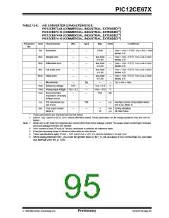
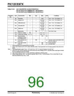
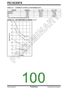
TABLE 12-9: A/D CONVERTER CHARACTERISTICS:
PIC12LCE673-04 (COMMERCIAL, INDUSTRIAL)
PIC12LCE674-04 (COMMERCIAL, INDUSTRIAL)
Parameter
No.
Sym Characteristic
Min
Typ†
Max
Units
Conditions
NR
Resolution
—
—
—
—
8-bits
—
—
VREF = VDD = 3.0V (Notes 1,4)
VREF = VDD = 3.0V (Notes 1,4)
NINT
Integral error
less than
±1 LSb
NDIF
NFS
Differential error
Full scale error
—
—
—
—
—
—
less than
±1 LSb
—
—
—
VREF = VDD = 3.0V (Notes 1,4)
VREF = VDD = 3.0V (Notes 1,4)
VREF = VDD = 3.0V (Notes 1,4)
VSS ≤ AIN ≤ VREF
less than
±1 LSb
NOFF Offset error
less than
±1 LSb
—
Monotonicity
—
Typ
—
—
—
V
VREF Reference voltage
TBD
VDD + 0.3
VREF + 0.3
10.0
VAIN
ZAIN
Analog input voltage VSS - 0.3
—
V
Recommended
—
—
kΩ
impedance of ana-
log voltage source
IAD
A/D conversion cur-
rent (VDD)
—
—
TBD
—
—
µA Average current consumption when
A/D is on. (Note 2)
IREF
VREF input current
(Note 3)
TBD
TBD
mA During sampling
µA All other times
*
These parameters are characterized but not tested.
†
Data in “Typ” column is at 5V, 25°C unless otherwise stated. These parameters are for design guidance only and are not
tested.
Note 1: These specifications apply if VREF = 3.0V and if VDD ≥ 3.0V. VIN must be between VSS and VREF
2: When A/D is off, it will not consume any current other than minor leakage current. The power-down current spec includes
any such leakage from the A/D module.
3: VREF current is from GP1 pin or VDD pin, whichever is selected as reference input.
4: When using external VREF, VDD must be greater than 3V for +1 LSB accuracy. If VDD is less than 3V, you
must use internal VREF for +1 LSB.
DS40181B-page 96
Preliminary
1998 Microchip Technology Inc.

 MICROCHIP [ MICROCHIP ]