PIC12CE67X
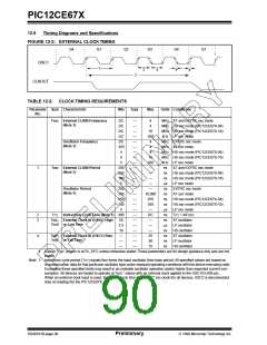
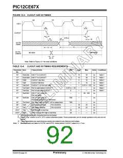
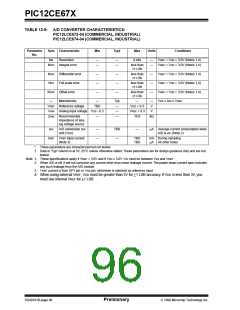
FIGURE 12-3: CLKOUT AND I/O TIMING
Q1
Q2
Q3
Q4
OSC1
11
10
CLKOUT
13
14
12
18
19
16
I/O Pin
(input)
15
17
I/O Pin
new value
old value
(output)
20, 21
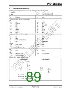
Note: Refer to Figure 12-1 for load conditions.
TABLE 12-4: CLKOUT AND I/O TIMING REQUIREMENTS
Parameter Sym
No.
Characteristic
Min
Typ†
Max
Units Conditions
10*
11*
12*
13*
14*
15*
16*
17*
TosH2ckL OSC1↑ to CLKOUT↓
TosH2ckH OSC1↑ to CLKOUT↑
—
—
—
—
—
15
15
5
30
ns
ns
ns
ns
ns
ns
ns
ns
Note 1
Note 1
Note 1
Note 1
Note 1
Note 1
Note 1
30
TckR
TckF
CLKOUT rise time
CLKOUT fall time
15
15
5
TckL2ioV CLKOUT ↓ to Port out valid
TioV2ckH Port in valid before CLKOUT ↑
—
—
—
—
0.5TCY + 20
—
0.25TCY + 25
TckH2ioI
Port in hold after CLKOUT ↑
0
—
TosH2ioV OSC1↑ (Q1 cycle) to
—
80 - 100
Port out valid
18*
TosH2ioI
OSC1↑ (Q2 cycle) to
TBD
—
—
ns
Port input invalid (I/O in hold time)
19*
20*
TioV2osH Port input valid to OSC1↑ (I/O in setup time)
TBD
—
—
10
10
—
—
—
25
25
—
—
ns
ns
ns
ns
ns
TioR
TioF
Tinp
Trbp
Port output rise time
Port output fall time
INT pin high or low time
PIC12CE67X
PIC12CE67X
21*
—
22††*
23††*
20
GPIO change INT high or low time
20
*
These parameters are characterized but not tested.
†
Data in "Typ" column is at 5V, 25°C unless otherwise stated. These parameters are for design guidance only and are not
tested.
†† These parameters are asynchronous events not related to any internal clock edges.
Note 1: Measurements are taken in EXTRC and INTRC modes where CLKOUT output is 4 x TOSC.
DS40181B-page 92
Preliminary
1998 Microchip Technology Inc.

 MICROCHIP [ MICROCHIP ]