PIC12CE67X
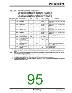
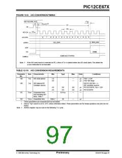
FIGURE 12-6: A/D CONVERSION TIMING
BSF ADCON0, GO
(TOSC/2) (1)
1 Tcy
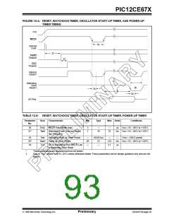
131
130
Q4
132
A/D CLK
7
6
5
4
3
2
1
0
A/D DATA
NEW_DATA
OLD_DATA
ADRES
ADIF
GO
DONE
SAMPLING STOPPED
SAMPLE
Note 1: If the A/D clock source is selected as RC, a time of TCY is added before the A/D clock starts. This allows the
SLEEPinstruction to be executed.
TABLE 12-10: A/D CONVERSION REQUIREMENTS
Parameter
No.
Sym Characteristic
Min
Typ†
Max
Units
Conditions
VREF ≥ 3.0V
130
TAD
TAD
A/D clock period
1.6
2.0
—
—
µs
µs VREF full range
130
A/D Internal RC
Oscillator source
ADCS1:ADCS0 = 11
(RC oscillator source)
3.0
2.0
—
6.0
4.0
9.0
6.0
—
µs PIC12LCE67X, VDD = 3.0V
µs PIC12CE67X
131
132
TCNV Conversion time
(not including S/H
time). Note 1
9.5TAD
—
TACQ Acquisition time
Note 2
20
—
µs
*
These parameters are characterized but not tested.
†
Data in “Typ” column is at 5V, 25°C unless otherwise stated. These parameters are for design guidance only and are not
tested.
Note 1: ADRES register may be read on the following TCY cycle.
1998 Microchip Technology Inc.
Preliminary
DS40181B-page 97

 MICROCHIP [ MICROCHIP ]