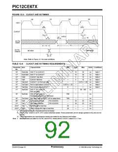
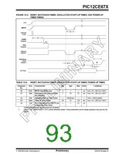
PIC12CE67X
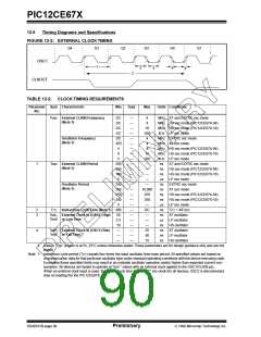
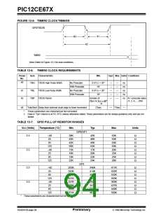
FIGURE 12-5: TIMER0 CLOCK TIMINGS
GP2/T0CKI
41
40
42
TMR0
Note: Refer to Figure 12-1 for load conditions.
TABLE 12-6: TIMER0 CLOCK REQUIREMENTS
Param
No.
Sym
Characteristic
Min
Typ† Max Units Conditions
40
Tt0H
T0CKI High Pulse Width
No Prescaler
With Prescaler
No Prescaler
With Prescaler
0.5TCY + 20*
10*
—
—
—
—
—
—
—
—
—
—
ns
ns
ns
ns
41
42
Tt0L
Tt0P
T0CKI Low Pulse Width
T0CKI Period
0.5TCY + 20*
10*
Greater of:
ns N = prescale value
(1, 2, 4,..., 256)
20µs or TCY + 40*
N
48
Tcke2tmrI Delay from external clock edge to timer increment
These parameters are characterized but not tested.
2Tosc
—
7Tosc
—
*
†
Data in "Typ" column is at 5V, 25°C unless otherwise stated. These parameters are for design guidance only and are not
tested.
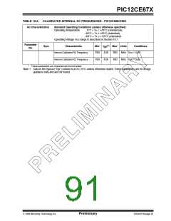
TABLE 12-7: GPIO PULL-UP RESISTOR RANGES
VDD (Volts)
Temperature (°C)
Min
Typ
Max
Units
GP0/GP1
2.5
–40
25
38K
42K
42K
50K
15K
18K
19K
22K
42K
48K
49K
55K
17K
20K
22K
24K
63K
63K
63K
63K
20K
23K
25K
28K
Ω
Ω
Ω
Ω
Ω
Ω
Ω
Ω
85
125
–40
25
5.5
85
125
GP3
2.5
5.5
–40
25
285K
343K
368K
431K
247K
288K
306K
351K
346K
414K
457K
504K
292K
341K
371K
407K
417K
532K
532K
593K
360K
437K
448K
500K
Ω
Ω
Ω
Ω
Ω
Ω
Ω
Ω
85
125
–40
25
85
125
*
These parameters are characterized but not tested.
DS40181B-page 94
Preliminary
1998 Microchip Technology Inc.

 MICROCHIP [ MICROCHIP ]