PIC12CE67X
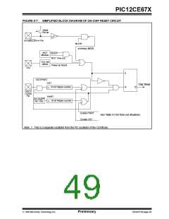
the chip in reset until the crystal oscillator is stable.The
other is the Power-up Timer (PWRT), which provides a
fixed delay of 72 ms (nominal) on power-up only,
designed to keep the part in reset while the power sup-
ply stabilizes. With these two timers on-chip, most
applications need no external reset circuitry.
9.0
SPECIAL FEATURES OF THE
CPU
What sets a microcontroller apart from other proces-
sors are special circuits to deal with the needs of real-
time applications. The PIC12CE67X family has a host
of such features intended to maximize system reliabil-
ity, minimize cost through elimination of external com-
ponents, provide power saving operating modes and
offer code protection. These are:
SLEEP mode is designed to offer a very low current
power-down mode.The user can wake-up from SLEEP
through external reset, Watchdog Timer Wake-up, or
through an interrupt. Several oscillator options are also
made available to allow the part to fit the application.
The EXTRC oscillator option saves system cost while
the LP crystal option saves power. A set of configura-
tion bits are used to select various options.
• Oscillator selection
• Reset
- Power-on Reset (POR)
- Power-up Timer (PWRT)
- Oscillator Start-up Timer (OST)
• Interrupts
9.1
Configuration Bits
The configuration bits can be programmed (read as '0')
or left unprogrammed (read as '1') to select various
device configurations. These bits are mapped in pro-
gram memory location 2007h.
• Watchdog Timer (WDT)
• SLEEP
• Code protection
• ID locations
The user will note that address 2007h is beyond the
user program memory space. In fact, it belongs to the
special test/configuration memory space (2000h-
3FFFh), which can be accessed only during
programming.
• In-circuit serial programming
The PIC12CE67X has a Watchdog Timer which can be
shut off only through configuration bits. It runs off its
own RC oscillator for added reliability. There are two
timers that offer necessary delays on power-up. One is
the Oscillator Start-up Timer (OST), intended to keep
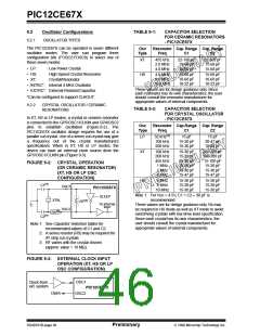
FIGURE 9-1: CONFIGURATION WORD
CP1 CP0 CP1 CP0 CP1 CP0 MCLRE CP1
bit13
CP0 PWRTE WDTE FOSC2 FOSC1 FOSC0
bit0
Register: CONFIG
Address
2007h
(1)
bit 13-8, CP1:CP0: Code Protection bit pairs
6-5: 11= Code protection off
10= Locations 400h through 7FEh code protected (do not use for PIC12CE673)
01= Locations 200h through 7FEh code protected
00= All memory is code protected
bit 7:
bit 4:
bit 3:
MCLRE: Master Clear Reset Enable bit
1 = Master Clear Enabled
0 = Master Clear Disabled
PWRTE: Power-up Timer Enable bit
1 = PWRT disabled
0 = PWRT enabled
WDTE: Watchdog Timer Enable bit
1 = WDT enabled
0 = WDT disabled
bit 2-0: FOSC2:FOSC0: Oscillator Selection bits
111= EXTRC, Clockout on OSC2
110= EXTRC, OSC2 is I/O
101= INTRC, Clockout on OSC2
100= INTRC, OSC2 is I/O
011= Invalid Selection
010= HS Oscillator
001= XT Oscillator
000= LP Oscillator
Note 1: All of the CP1:CP0 pairs have to be given the same value to enable the code protection scheme listed.
1998 Microchip Technology Inc.
Preliminary
DS40181B-page 45

 MICROCHIP [ MICROCHIP ]