PIC12CE67X
8.2
Selecting the A/D Conversion Clock
8.3
Configuring Analog Port Pins
The A/D conversion time per bit is defined as TAD. The
A/D conversion requires 9.5 TAD per 8-bit conversion.
The source of the A/D conversion clock is software
selected. The four possible options for TAD are:
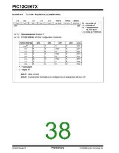
The ADCON1 and TRIS registers control the operation
of the A/D port pins. The port pins that are desired as
analog inputs must have their corresponding TRIS bits
set (input). If the TRIS bit is cleared (output), the digital
output level (VOH or VOL) will be converted.
• 2TOSC
The A/D operation is independent of the state of the
CHS2:CHS0 bits and the TRIS bits.
• 8TOSC
• 32TOSC
• Internal ADC RC oscillator
Note 1: When reading the port register, all pins
configured as analog input channel will
read as cleared (a low level). Pins config-
ured as digital inputs, will convert an ana-
log input. Analog levels on a digitally
configured input will not affect the conver-
sion accuracy.
For correct A/D conversions, the A/D conversion clock
(TAD) must be selected to ensure a minimum TAD time
of 1.6 µs.
Table 8-1 shows the resultant TAD times derived from
the device operating frequencies and the A/D clock
source selected.
Note 2: Analog levels on any pin that is defined as
a digital input (including the AN3:AN0
pins), may cause the input buffer to con-
sume current that is out of the devices
specification.
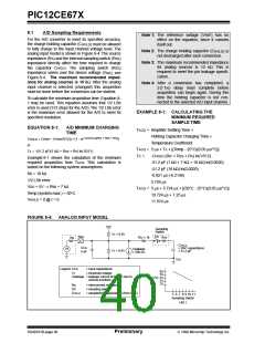
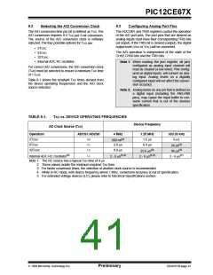
TABLE 8-1:
TAD vs. DEVICE OPERATING FREQUENCIES
Device Frequency
AD Clock Source (TAD)
ADCS1:ADCS0
Operation
2TOSC
4 MHz
1.25 MHz
1.6 µs
333.33 kHz
(2)
00
01
10
11
6 µs
500 ns
(3)
8TOSC
2.0 µs
6.4 µs
24 µs
(3)
(3)
32TOSC
8.0 µs
25.6 µs
96 µs
(5)
(1,4)
(1,4)
(1)
Internal ADC RC Oscillator
2 - 6 µs
2 - 6 µs
2 - 6 µs
Note 1: The RC source has a typical TAD time of 4 µs.
2: These values violate the minimum required TAD time.
3: For faster conversion times, the selection of another clock source is recommended.
4: While in RC mode, with device frequency above 1 MHz, conversion accuracy is out of specification.
5: For extended voltage devices (LC), please refer to Electrical Specifications section.
1998 Microchip Technology Inc.
Preliminary
DS40181B-page 41

 MICROCHIP [ MICROCHIP ]