PIC12CE67X
9.2.5
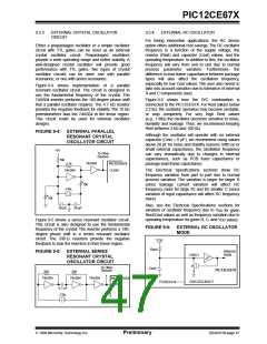
INTERNAL 4 MHz RC OSCILLATOR
9.3
Reset
The PIC12CE67X differentiates between various kinds
of reset:
The internal RC oscillator provides a fixed 4 MHz (nom-
inal) system clock at VDD = 5V and 25°C, see "Electri-
cal Specifications" section for information on variation
over voltage and temperature.
• Power-on Reset (POR)
• MCLR reset during normal operation
• MCLR reset during SLEEP
• WDT Reset (normal operation)
In addition, a calibration instruction is programmed into
the last address of the program memory which contains
the calibration value for the internal RC oscillator. This
value is programmed as a RETLW XXinstruction where
XX is the calibration value. In order to retrieve the cali-
bration value, issue a CALL YYinstruction where YY is
the last location in program memory (03FFh for the
PIC12CE673, 07FFh for the PIC12CE674). Control will
be returned to the user’s program with the calibration
value loaded into the W register. The program should
then perform a MOVWF OSCCAL instruction to load
the value into the internal RC oscillator trim register.
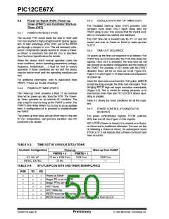
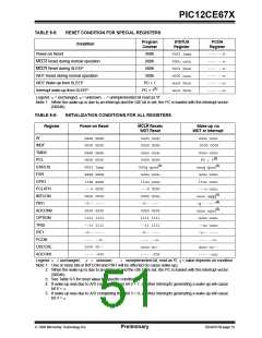
Some registers are not affected in any reset condition;
their status is unknown on POR and unchanged in any
other reset. Most other registers are reset to a “reset
state” on Power-on Reset (POR), MCLR Reset, WDT
Reset, and MCLR Reset during SLEEP. They are not
affected by a WDT Wake-up, which is viewed as the
resumption of normal operation. The TO and PD bits
are set or cleared differently in different reset situations
as indicated in Table 9-4. These bits are used in
software to determine the nature of the reset. See
Table 9-5 for a full description of reset states of all
registers.
OSCCAL, when written to with the calibration value, will
“trim” the internal oscillator to remove process variation
from the oscillator frequency. Only bits <7:2> of OSC-
CAL are implemented, and bits <1:0> should be written
as 0 for compatibility with future devices. The oscillator
calibration location is not code protected.
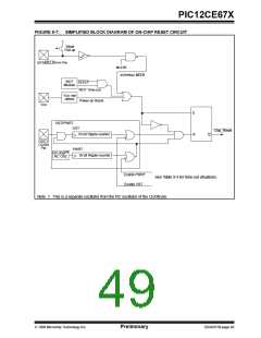
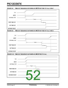
A simplified block diagram of the on-chip reset circuit is
shown in Figure 9-7.
The PIC12CE67X has a MCLR noise filter in the MCLR
reset path.The filter will detect and ignore small pulses.
Note: Please note that erasing the device will
also erase the pre-programmed internal
calibration value for the internal oscillator.
The calibration value must be saved prior
to erasing the part.
It should be noted that a WDT Reset does not drive
MCLR pin low.
9.2.6
CLKOUT
The PIC12CE67X can be configured to provide a clock
out signal (CLKOUT) on pin 3 when the configuration
word address (2007h) is programmed with FOSC2,
FOSC1, FOSC0 equal to 101 for INTRC or 111 for
EXTRC. The oscillator frequency, divided by 4 can be
used for test purposes or to synchronize other logic.
DS40181B-page 48
Preliminary
1998 Microchip Technology Inc.

 MICROCHIP [ MICROCHIP ]