PIC12CE67X
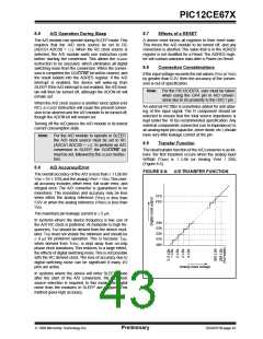
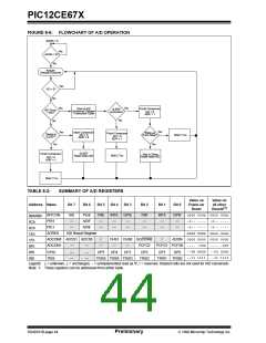
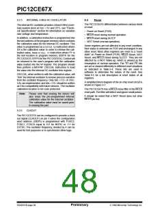
FIGURE 8-6: FLOWCHART OF A/D OPERATION
ADON = 0
Yes
ADON = 0?
No
Acquire
Selected Channel
Yes
GO = 0?
No
Yes
Yes
Start of A/D
Conversion Delayed
1 Instruction Cycle
Finish Conversion
SLEEP
Instruction?
A/D Clock
= RC?
GO = 0
ADIF = 1
No
No
Yes
Yes
Abort Conversion
GO = 0
Wake-up
From Sleep?
Finish Conversion
Device in
SLEEP?
Wait 2 TAD
GO = 0
ADIF = 1
ADIF = 0
No
No
SLEEP
Power-down A/D
Finish Conversion
Stay in Sleep
Power-down A/D
Wait 2 TAD
GO = 0
ADIF = 1
Wait 2 TAD
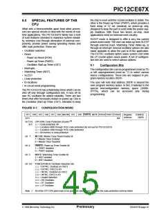
TABLE 8-2:
SUMMARY OF A/D REGISTERS
Value on
Power-on
Reset
Value on
all other
Resets
Address Name
Bit 7
Bit 6
Bit 5
Bit 4
Bit 3
Bit 2
Bit 1
Bit 0
(1)
INTCON
GIE
—
PEIE
ADIF
ADIE
T0IE
—
INTE GPIE
T0IF
—
INTF
—
GPIF
—
0000 000x 0000 000u
-0-- ---- -0-- ----
-0-- ---- -0-- ----
xxxx xxxx uuuu uuuu
0Bh/8Bh
0Ch
8Ch
1Eh
PIR1
—
—
—
—
PIE1
—
—
—
—
—
ADRES
A/D Result Register
ADCON0 ADCS1 ADCS0
r
CHS1 CHS0 GO/DONE
r
ADON 0000 0000 0000 0000
1Fh
ADCON1
—
—
—
—
—
PCFG2
PCFG1 PCFG0 ---- -000 ---- -000
9Fh
--xx xxxx --uu uuuu
--11 1111 --11 1111
05h
GPIO
TRIS
—
—
—
—
GP5
GP4
GP3
GP2
GP1
GP0
85h
TRIS5 TRIS4 TRIS3
TRIS2
TRIS1
TRIS0
Legend: x= unknown, u= unchanged, -= unimplemented read as '0', r = reserved. Shaded cells are not used for A/D conversion.
Note 1: These registers can be addressed from either bank.
DS40181B-page 44
Preliminary
1998 Microchip Technology Inc.

 MICROCHIP [ MICROCHIP ]