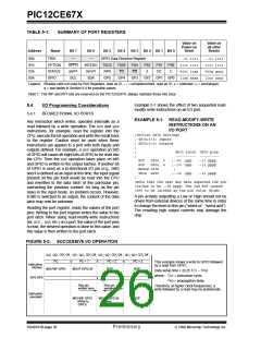
PIC12CE67X
rewritten. To use
a
port pin as output, the
5.0
I/O PORT
corresponding direction control bit in TRIS must be
cleared (= 0). For use as an input, the corresponding
TRIS bit must be set. Any I/O pin (except GP3) can be
programmed individually as input or output.
As with any other register, the I/O register can be
written and read under program control. However,
read instructions (e.g., MOVF GPIO,W) always read the
I/O pins independent of the pin’s input/output modes.
On RESET, all I/O ports are defined as input (inputs
are at hi-impedance) since the I/O control registers are
all set.
Port pins GP6 and GP7 are used for the serial
EEPROM interface. These port pins are not available
externally on the package. Users should avoid writing
to pins GP6 and GP7 when not communicating with
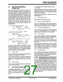
the serial EEPROM memory. Please see section 6.0,
EEPROM Peripheral Operation, for information on
serial EEPROM communication.
5.1
GPIO
GPIO is an 8-bit I/O register. Only the low order 6 bits
are used (GP5:GP0). Bits 6 and 7 (SDA and SCL) are
used by the EEPROM peripheral. Refer to Section 6.0
and Appendix A for use of SDA and SCL. Please note
that GP3 is an input only pin. The configuration word
can set several I/O’s to alternate functions. When
acting as alternate functions the pins will read as ‘0’
during port read. Pins GP0, GP1, and GP3 can be
configured with weak pull-ups and also with interrupt
on change. The interrupt on change and weak pull-up
functions are not pin selectable. If pin 4 is configured
as MCLR, the weak pull-up is always on. Interrupt on
change for this pin is not set and GP3 will read as '0'.
Interrupt on change is enabled by setting INTCON<3>.
Note that external oscillator use overrides the GPIO
functions on GP4 and GP5.
Note:
On a Power-on Reset, GP0, GP1, GP2,
GP4 are configured as analog inputs and
read as '0'.
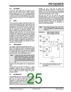
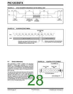
FIGURE 5-1: EQUIVALENT CIRCUIT
FOR A SINGLE I/O PIN
Data
Bus
D
Q
Q
Data
VDD
P
WR
Port
Latch
CK
5.2
TRIS Register
N
I/O
pin(1)
W
Reg
This register controls the data direction for GPIO. A '1'
from a TRIS register bit puts the corresponding output
driver in a hi-impedance mode. A '0' puts the contents
of the output data latch on the selected pins, enabling
the output buffer. The exceptions are GP3 which is
input only and its TRIS bit will always read as '1'.
D
Q
Q
TRIS
Latch
VSS
TRIS ‘f’
CK
Reset
Note:
A read of the ports reads the pins, not the
output data latches. That is, if an output
driver on a pin is enabled and driven high,
but the external system is holding it low, a
read of the port will indicate that the pin is
low.
RD Port
Note 1: I/O pins have protection diodes to VDD and VSS.
Upon reset, the TRIS register is all '1's, making all pins
inputs.
GP3 is input only with no data latch and no
output drivers.
TRIS for pins GP4 and GP5 is forced to a 1 where
appropriate. Writes to TRIS <5:4> will have an effect
in EXTRC and INTRC oscillator modes only. When
GP4 is configured as CLKOUT, changes to TRIS<4>
will have no effect.
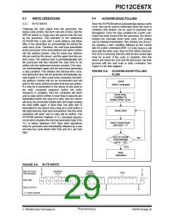
5.3
I/O Interfacing
The equivalent circuit for an I/O port pin is shown in
Figure 5-2. All port pins, except GP3 which is input
only, may be used for both input and output
operations. For input operations these ports are non-
latching. Any input must be present until read by an
input instruction (e.g., MOVF GPIO,W). The outputs are
latched and remain unchanged until the output latch is
1998 Microchip Technology Inc.
Preliminary
DS40181B-page 25

 MICROCHIP [ MICROCHIP ]