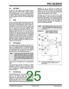
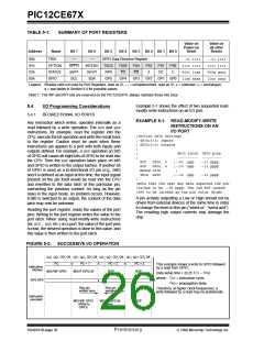
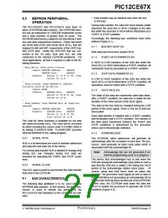
PIC12CE67X
6.3
WRITE OPERATIONS
6.4
ACKNOWLEDGE POLLING
6.3.1
BYTE WRITE
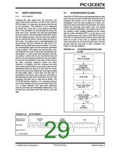
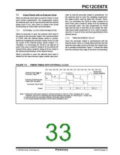
Since the EEPROM will not acknowledge during a write
cycle, this can be used to determine when the cycle is
complete (this feature can be used to maximize bus
throughput). Once the stop condition for a write com-
mand has been issued from the processor, the device
initiates the internally timed write cycle. ACK polling
can be initiated immediately. This involves the proces-
sor sending a start condition followed by the control
byte for a write command (R/W = 0). If the device is still
busy with the write cycle, then no ACK will be returned.
If no ACK is returned, then the start bit and control byte
must be re-sent. If the cycle is complete, then the
device will return the ACK and the processor can then
proceed with the next read or write command. See
Figure 6-4 for flow diagram.
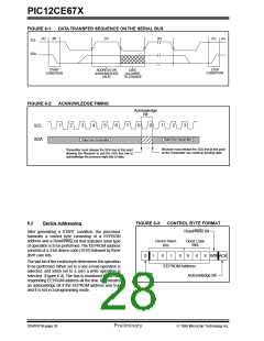
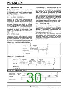
Following the start signal from the processor, the
device code (4 bits), the don't care bits (3 bits), and the
R/W bit (which is a logic low) are placed onto the bus
by the processor. This indicates to the addressed
EEPROM that a byte with a word address will follow
after it has generated an acknowledge bit during the
ninth clock cycle. Therefore, the next byte transmitted
by the processor is the word address and will be written
into the address pointer. Only the lower four address
bits are used by the device, and the upper four bits are
don’t cares. The address byte is acknowledgeable and
the processor will then transmit the data word to be
written into the addressed memory location. The mem-
ory acknowledges again and the processor generates
a stop condition. This initiates the internal write cycle,
and during this time will not generate acknowledge sig-
nals (Figure 6-5). After a byte write command, the inter-
nal address counter will not be incremented and will
point to the same address location that was just written.
If a stop bit is transmitted to the device at any point in
the write command sequence before the entire
sequence is complete, then the command will abort
and no data will be written. If more than 8 data bits are
transmitted before the stop bit is sent, then the device
will clear the previously loaded byte and begin loading
the data buffer again. If more than one data byte is
transmitted to the device and a stop bit is sent before a
full eight data bits have been transmitted, then the write
command will abort and no data will be written. The
EEPROM memory employs a VCC threshold detector
circuit which disables the internal erase/write logic if the
VCC is below minimum VDD. Byte write operations
must be preceded and immediately followed by a bus
not busy bus cycle where both SDA and SCL are held
high.
FIGURE 6-4: ACKNOWLEDGE POLLING
FLOW
Send
Write Command
Send Stop
Condition to
Initiate Write Cycle
Send Start
Send Control Byte
with R/W = 0
Did EEPROM
NO
Acknowledge
(ACK = 0)?
YES
Next
Operation
FIGURE 6-5: BYTE WRITE
S
T
A
R
T
S
T
O
P
BUS ACTIVITY
PROCESSOR
CONTROL
BYTE
WORD
ADDRESS
DATA
SDA LINE
P
S
1
0
1
0
X
X
X
0
X
X
X X
A
C
K
A
C
K
A
C
K
BUS ACTIVITY
X = Don’t Care Bit
1998 Microchip Technology Inc.
Preliminary
DS40181B-page 29

 MICROCHIP [ MICROCHIP ]