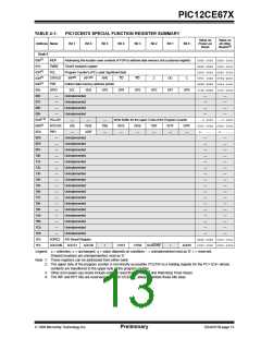
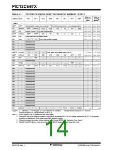
PIC12CE67X
4.2.2.3
INTCON REGISTER
Note: Interrupt flag bits get set when an interrupt
condition occurs regardless of the state of
its corresponding enable bit or the global
enable bit, GIE (INTCON<7>).
The INTCON Register is a readable and writable regis-
ter which contains various enable and flag bits for the
TMR0 register overflow, GPIO Port change and Exter-
nal GP2/INT Pin interrupts.
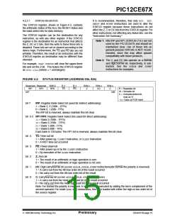
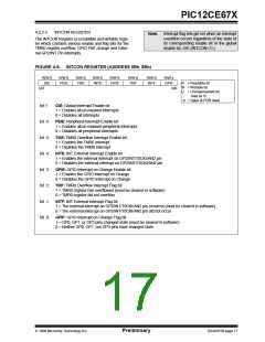
FIGURE 4-5: INTCON REGISTER (ADDRESS 0Bh, 8Bh)
R/W-0
GIE
R/W-0
PEIE
R/W-0
T0IE
R/W-0
INTE
R/W-0
GPIE
R/W-0
T0IF
R/W-0
INTF
R/W-x
GPIF
R
= Readable bit
W = Writable bit
bit7
bit0
U
= Unimplemented bit,
read as ‘0’
- n = Value at POR reset
bit 7:
GIE: Global Interrupt Enable bit
1 = Enables all un-masked interrupts
0 = Disables all interrupts
bit 6:
bit 5:
bit 4:
bit 3:
bit 2:
bit 1:
bit 0:
PEIE: Peripheral Interrupt Enable bit
1 = Enables all un-masked peripheral interrupts
0 = Disables all peripheral interrupts
T0IE: TMR0 Overflow Interrupt Enable bit
1 = Enables the TMR0 interrupt
0 = Disables the TMR0 interrupt
INTE: INT External Interrupt Enable bit
1 = Enables the external interrupt on GP2/INT/T0CKI/AN2 pin
0 = Disables the external interrupt on GP2/INT/T0CKI/AN2 pin
GPIE: GPIO Interrupt on Change Enable bit
1 = Enables the GPIO Interrupt on Change
0 = Disables the GPIO Interrupt on Change
T0IF: TMR0 Overflow Interrupt Flag bit
1 = TMR0 register has overflowed (must be cleared in software)
0 = TMR0 register did not overflow
INTF: INT External Interrupt Flag bit
1 = The external interrupt on GP2/INT/T0CKI/AN2 pin occurred (must be cleared in software)
0 = The external interrupt on GP2/INT/T0CKI/AN2 pin did not occur
GPIF: GPIO Interrupt on Change Flag bit
1 = GP0, GP1, or GP3 pins changed state (must be cleared in software)
0 = Neither GP0, GP1, nor GP3 pins have changed state
1998 Microchip Technology Inc.
Preliminary
DS40181B-page 17

 MICROCHIP [ MICROCHIP ]