PIC12CE67X
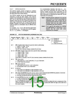
4.2.2.2
OPTION REGISTER
Note: To achieve a 1:1 prescaler assignment for
the TMR0 register, assign the prescaler to
the Watchdog Timer by setting bit PSA
(OPTION<3>).
The OPTION register is a readable and writable regis-
ter which contains various control bits to configure the
TMR0/WDT prescaler, the External INT Interrupt,
TMR0, and the weak pull-ups on GPIO.
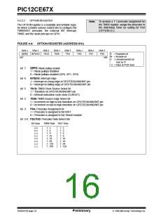
FIGURE 4-4: OPTION REGISTER (ADDRESS 81h)
R/W-1
GPPU
R/W-1
R/W-1
T0CS
R/W-1
T0SE
R/W-1
PSA
R/W-1
PS2
R/W-1
PS1
R/W-1
PS0
INTEDG
R
= Readable bit
W = Writable bit
U
bit7
bit0
= Unimplemented bit,
read as ‘0’
- n = Value at POR reset
bit 7:
bit 6:
bit 5:
bit 4:
bit 3:
GPPU: Weak pullup enable
1 = Weak pullups disabled
0 = Weak pullups enabled (GP0, GP1, GP3)
INTEDG: Interrupt edge
1 = Interrupt on rising edge of GP2/T0CKI/AN2/INT pin
0 = Interrupt on falling edge of GP2/T0CKI/AN2/INT pin
T0CS: TMR0 Clock Source Select bit
1 = Transition on GP2/T0CKI/AN2/INT pin
0 = Internal instruction cycle clock (CLKOUT)
T0SE: TMR0 Source Edge Select bit
1 = Increment on high-to-low transition on GP2/T0CKI/AN2/INT pin
0 = Increment on low-to-high transition on GP2/T0CKI/AN2/INT pin
PSA: Prescaler Assignment bit
1 = Prescaler is assigned to the WDT
0 = Prescaler is assigned to the Timer0 module
bit 2-0: PS2:PS0: Prescaler Rate Select bits
Bit Value
TMR0 Rate WDT Rate
000
001
010
011
100
101
110
111
1 : 2
1 : 4
1 : 8
1 : 16
1 : 32
1 : 64
1 : 128
1 : 256
1 : 1
1 : 2
1 : 4
1 : 8
1 : 16
1 : 32
1 : 64
1 : 128
DS40181B-page 16
Preliminary
1998 Microchip Technology Inc.

 MICROCHIP [ MICROCHIP ]