KSZ8795CLX
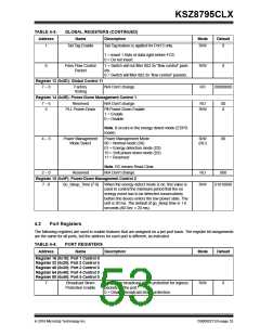
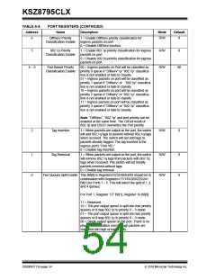
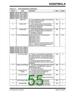
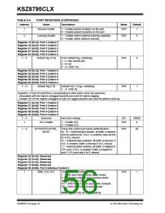
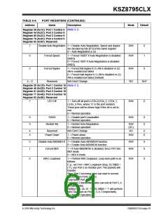
TABLE 4-4:
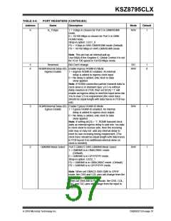
Address
6
PORT REGISTERS (CONTINUED)
Name
Description
Mode
Default
Is_1Gbps
1 = 1Gbps is chosen for Port 5 in GMII/RGMII
mode.
R/W
1
0 = 10/100 Mbps is chosen for Port 5 in GMII/
RGMII mode.
Strap-in option: LED1_0
PU = 1Gbps in SW5-GMII/RGMII mode (Default)
PD = 10/100 Mbps in SW5-GMII/RGMII mode
Note: This pin has an internal pull-up.
Use Bit[4] of the Register 6, Global Control 4 to set
for 10 or 100 speed in 10/100 Mbps mode.
5
4
Reserved
N/A Don’t change.
RO
1
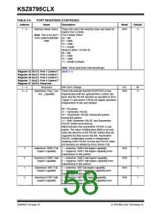
0
RGMII Internal Delay (ID) Enable Ingress RGMII-ID Mode
Ingress Enable 1 = Ingress RGMII-ID enabled. An internal
R/W
delay is added to ingress clock input.
0 = No delay is added, only clock to data
skew applied.
Note: If RGMII connection partner transmit data to
clock skew is in standard spec ±0.5 ns without
delay inserted on PCB, then set bit [4] =’1’ will
enable an ingress delay to meet the input skew min
1ns to max 2.6 ns requirement (the clock trace
should be equal length with data traces in PCB lay-
out).
3
RGMII Internal Delay (ID) Enable Egress RGMII-ID Mode
Egress Enable 1 = Egress RGMII-ID enabled. An internal
R/W
1
delay is added to egress clock output.
0 = No delay is added, only clock to data
skew applied.
Note: If setting bit [3] = ‘1’, RGMII transmit clock
adds an internal egress delay to add min 1ns data
to clock skew to receive side, then the receiving
side may or may not add any internal delay to
meet its own receiving timing requirement. (The
clock trace should be equal length with data traces
in PCB layout if no additional external skew on
clock is needed).
2
GMII/MII Mode Select Port 5 GMAC5 SW5-GMII/MII Mode Select
1 = GMII/MII is in GMAC/MAC mode
(Default).
R/W
1
0 = GMII/MII is in GPHY/PHY mode.
Strap-in option: LED2_1
PU = GMII/MII is in GMAC/MAC mode. (Default)
PD = GMII/MII is in GPHY/PHY mode.
Note: When set GMAC5 SW5-GMII to GPHY
mode, the CRS and COL pins will change from the
input to output.
When set SW5-MII to PHY mode, the CRS, COL,
RXC and TXC pins will change from the input to
output.
2016 Microchip Technology Inc.
DS00002112A-page 57

 MICREL [ MICREL SEMICONDUCTOR ]