KSZ8795CLX
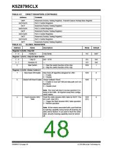
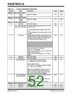
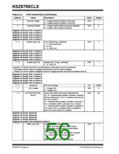
TABLE 4-3:
Address
GLOBAL REGISTERS (CONTINUED)
Name
Description
Mode
Default
Register 9 (0x09): Global Control 7
7 - 0
Factory
Testing
N/A Don’t Change
RO
0x40
Register 10 (0x0A): Global Control 8
7 - 0
Factory
Testing
N/A Don’t Change
N/A Don’t Change
RO
0x00
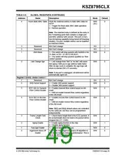
Register 11 (0x0B): Global Control 9
7
6
Reserved
RO
0
0
Port 5 SW5- RMII Refer- Select the data sampling edge of the SW5- RMII
ence Clock Edge Select reference clock:
R/W
1 = Data sampling on the negative edge of REF-
CLK.
0 = Data sampling on the positive edge of REFCLK
(default).
5 4
LED Mode
Programmable LED output to indicate port’s activ-
ity/status using 2 bits of the control register. LED is
ON (active) when the output is LOW; the LED is
OFF (inactive) when the output is HIGH.
R/W
00
LINK = LED ON; ACT = LED Blink;
LINK/ACT = LED On/Blink.
Speed = LED ON (100BT); LED OFF (10BT); LED
Blink (1000BT reserved).
Duplex = LED ON (Full duplex); LED OFF (half
duplex).
3
2
1
Reserved
Reserved
N/A Don’t change.
N/A Don’t change.
RO
RO
0
0
0
REFCLKO Enable
1 = Enable REFCLKO pin clock output
0 = Disable REFCLKO pin clock output.
R/W
Strap-in option: LED2_0
PU = REFCLK_O (25 MHz) is enabled. (Default)
PD = REFCLK_O is disabled
Note: This is an additional clock; this clock can
save an oscillator if system needs this clock
source. If the system doesn’t need this 25 MHz
clock source, which should be disabled.
0
SPI Read Sampling
Clock Edge Select
Select the SPI clock edge for sampling SPI read
data.
R/W
0
1 = Trigger on the rising edge of SPI clock (for
higher speed SPI)
0 = Trigger on the falling edge of SPI clock.
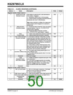
Register 12 (0x0C): Global Control 10
7 6
5 2
Reserved
Reserved
Reserved
RO
RO
01
N/A Don’t change.
0001
DS00002112A-page 52
2016 Microchip Technology Inc.

 MICREL [ MICREL SEMICONDUCTOR ]