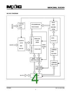
MX26L3220
RESET OPERATION
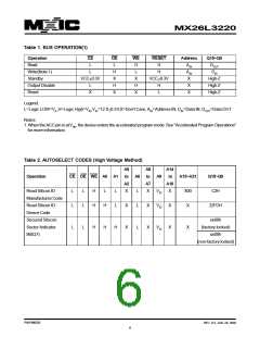
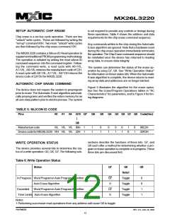
Table 3
VCC / VI/O Voltage Range
The RESET pin provides a hardware method of resetting
the device to reading array data.When the RESET pin is
driven low for at least a period of tRP, the device
immediately terminates any operation in progress,
tristates all output pins, and ignores all read/write
commands for the duration of the RESET pluse. The
device also resets the internal state machine to reading
array data.The operation that was interrupted should be
reinitated once the device is ready to accept another
command sequence, to ensure data integrity
Part No.
VCC=2.7V to 3.6VVCC=2.7V to 3.6V
VI/O=2.7V to 3.6VVI/O=1.65V to 2.6V
MX26L3220-90
MX26L3220-12
90ns
100ns
130ns
120ns
Notes: Typical values measured atVCC=2.7V to 3.6V,
VI/O=2.7V to 3.6V
Current is reduced for the duration of the RESET pulse.
When RESET is held at VSS±0.3V, the device draws
CMOS standby current (ICC4). If RESET is held at VIL
but not within VSS±0.3V, the standby current will be
greater.
DATA PROTECTION
The MX26L3220 is designed to offer protection against
accidental erasure or programming caused by spurious
system level signals that may exist during power transi-
tion. During power up the device automatically resets
the state machine in the Read mode. In addition, with
its control register architecture, alteration of the memory
contents only occurs after successful completion of spe-
cific command sequences. The device also incorporates
several features to prevent inadvertent write cycles re-
sulting fromVCC power-up and power-down transition or
system noise.
The RESET pin may be tied to system reset circuitry. A
system reset would that also reset the MTP EPROM.
Refer to the AC Characteristics tables for RESET
parameters and to Figure 14 for the timing diagram.
SILICON ID READ OPERATION
MTP EPROM are intended for use in applications where
the local CPU alters memory contents. As such, manu-
facturer and device codes must be accessible while the
device resides in the target system. EPROM program-
mers typically access signature codes by raising A9 to
a high voltage. However, multiplexing high voltage onto
address lines is not generally desired system design prac-
tice.
SECURED SILICON SECTOR
The MX26L3220 features a Flash memory region where
the system may access through a command sequence
to create a permant part identification as so called Elec-
tronic Serial Number (ESN) in the device. Once this re-
gion is programmed, any further modification on the re-
gion is impossible. The secured silicon sector is a 512
words in length, and uses a Secured Silicon Sector Indi-
cator Bit (Q7) to indicate whether or not the Secured
Silicon Sector is locked when shipped from the factory.
This bit is permanently set at the factory and cannot be
changed, which prevent duplication of a factory locked
part.This ensures the security of the ESN once the prod-
uct is shipped to the field.
MX26L3220 provides hardware method to access the
silicon ID read operation.Which method requiresVID on
A9 pin, VIL on CE, OE, A6, and A1 pins. Which apply
VIL on A0 pin, the device will output MXIC's manufac-
ture code of C2H.Which applyVIH on A0 pin, the device
will output MX26L3220 device code of 22FDH.
The MX26L3220 offers the device with Secured Silicon
Sector either factory locked or custor lockable.The fac-
tory-locked version is always protected when shipped
from the factory , and has the Secured Silicon Sector
Indicator Bit permanently set to a "1". The customer-
lockable version is shipped with the Secured Silicon
Sector unprotected, allowing customer to utilize that sec-
tor in any form they prefer.The customer-lockable ver-
VI/O PIN OPERATION
MX26L3220 is capable to provide the I/O prower supply
(VI/O) pin to control Input/Output voltage levels of the
device.The data outputs and voltage tolerated at its data
input is determined by the voltage on the VI/O pin.This
device is allows to operate in 1.8V or 3V system as re-
quired.
P/N:PM0826
REV. 0.5, JAN. 29, 2002
8

 Macronix [ MACRONIX INTERNATIONAL ]