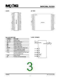
MX26L3220
REQUIREMENTS FOR READING ARRAY
DATA
STANDBY MODE
MX26L3220 can be set into Standby mode with two dif-
ferent approaches. One is using both CE and RESET
pins and the other one is using RESET pin only.
To read array data from the outputs, the system must
drive the CE and OE pins toVIL.CE is the power control
and selects the device. OE is the output control and gates
array data to the output pins.WE should remain at VIH.
When using both pins of CE and RESET, a CMOS
Standby mode is achieved with both pins held at Vcc ±
0.3V. Under this condition, the current consumed is less
than 50uA (typ.). If both of the CE and RESET are held
atVIH, but not within the range ofVCC ± 0.3V, the device
will still be in the standby mode, but the standby currect
will be larger. During Auto Algorithm operation, Vcc ac-
tive current (Icc2) is required even CE = "H" until the
operation is complated.The device can be read with stan-
dard access time (tCE) from either of these standby
modes.
The internal state machine is set for reading array data
upon device power-up, or after a hardware reset. This
ensures that no spurious alteration of the memory contect
occurs during the power transition. No command is
necessary in this mode to obtain array data. Standard
microprocessor read cycles that assert valid address on
the device address inputs produce valid data on the device
data outputs.The device remains enabled for read access
until the command register contents are altered.
When using only RESET, a CMOS standby mode is
achieved with RESET input held at Vss ±0.3V, Under
this condition the current is consumed less than 50uA
(typ.). Once the RESET pin is taken high,the device is
back to active without recovery delay.
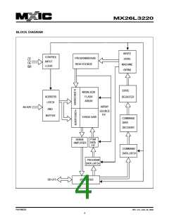
WRITE COMMANDS/COMMAND
SEQUENCES
To program data to the device the system must drive
WE and CE to VIL, and OE to VIH.
In the standby mode the outputs are in the high imped-
ance state, independent of the OE input.
An erase operation can erase the entire device. The
"Writing specific address and data commands or
sequences into the command register initiates device
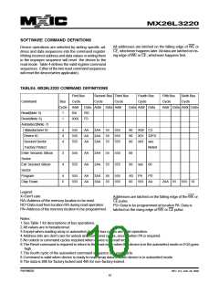
operations. Table 1 defines the valid register command
sequences.Writing incorrect address and data values or
writing them in the improper sequence resets the device
to reading array data."section has details on erasing the
entire chip.
MX26L3220 is capable to provide the Automatic Standby
Mode to restrain power consumption during read-out of
data.This mode can be used effectively with an applica-
tion requested low power consumption such as handy
terminals.
To active this mode, MX26L3220 automatically switch
themselves to low power mode when MX26L3220 ad-
dresses remain stable during access time of tACC+30ns.
It is not necessary to control CE, WE, and OE on the
mode. Under the mode, the current consumed is typi-
cally 50uA (CMOS level).
After the system writes the autoselect command
sequence, the device enters the autoselect mode. The
system can then read autoselect codes from the internal
reqister (which is separate from the memory array) on
Q15-Q0. Standard read cycle timings apply in this mode.
Refer to the Autoselect Mode and Autoselect Command
Sequence section for more information.
OUTPUT DISABLE
ICC2 in the DC Characteristics table represents the active
current specification for the write mode. The "AC
Characteristics" section contains timing specification
table and timing diagrams for write operations.
With the OE input at a logic high level (VIH), output from
the devices are disabled.This will cause the output pins
to be in a high impedance state.
P/N:PM0826
REV. 0.5, JAN. 29, 2002
7

 Macronix [ MACRONIX INTERNATIONAL ]