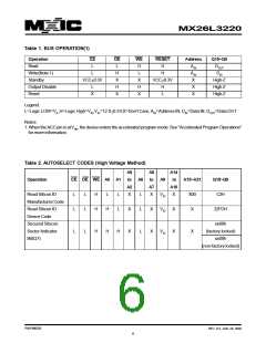
MX26L3220
SOFTWARE COMMAND DEFINTIONS
All addresses are latched on the falling edge of WE or
CE, whichever happens later.All data are latched on ris-
ing edge of WE or CE, whichever happens first.
Device operations are selected by writing specific ad-
dress and data sequences into the command register.
Writing incorrect address and data values or writing them
in the improper sequence will reset the device to the
read mode. Table 4 defines the valid register command
sequences. Either of the two reset command sequences
will reset the device(when applicable).
TABLE4. MX26L3220 COMMAND DEFINITIONS
First Bus
Cycle
Addr
Second Bus Third Bus
Cycle Cycle
Fourth Bus
Cycle
Fifth Bus
Cycle
Sixth Bus
Cycle
Command
Bus
Cycle
1
Data Addr Data Addr
Data Addr Data
Addr Data Addr Data
Read(Note 5)
Reset(Note 6)
Autoselect(Note 7)
Manufacturer ID
Device ID
RA
RD
F0
1
XXX
4
4
4
555
555
555
AA
2AA
2AA
2AA
55
55
55
555
555
555
90
90
90
X00 C2
X01 22FD
x03 see
Note9
AA
AA
Secured Sector
Factory Protect
Enter Secured Silicon
Sector
3
4
555
555
AA
AA
2AA
2AA
55
55
555
555
88
90
Exit Secured Silicon
Sector
xxx
PA
00
Porgram
4
6
555
555
AA
AA
2AA
2AA
55
55
555
555
A0
80
PD
Chip Erase
555 AA
2AA 55
555 10
Legend:
X=Don't care
RA=Address of the memory location to be read.
Addresses are latched on the falling edge of the WE or
CE pulse.
RD=Data read from location RA during read operation.
PA=Address of the memory location to be programmed.
PD=Data to be programmed at location PA. Data is
latched on the rising edge of WE or CE pulse.
Notes:
1.See Table 1 for descriptions of bus operations.
2.All values are in hexadecimal.
3.Except when reading array or autoselect data, all bus cycles are write operation.
4.Address bits are don't care for unlock and command cycles, except when PA is required.
5.No unlock or command cycles required when device is in read mode.
6.The Reset command is required to return to the read mode when the device is in the autoselect mode or if Q5 goes
high.
7.The fourth cycle of the autoselect command sequence is a read cycle.
8.Command is valid when device is ready to read array data or when device is in autoselect mode.
9.The data is 88h for factory locked and 48h for non-factory locked.
P/N:PM0826
REV. 0.5, JAN. 29, 2002
10

 Macronix [ MACRONIX INTERNATIONAL ]