MX26L3220
SETUP AUTOMATIC CHIP ERASE
is not required to provide any controls or timings during
these operations. Table 4 shows the address and data
requirements for the chip erase command sequence.
Chip erase is a six-bus cycle operation. There are two
"unlock" write cycles. These are followed by writing the
"set-up" command 80H. Two more "unlock" write cycles
are then followed by the chip erase command 10H.
Any commands written to the chip during the Automatic
Erase algorithm are ignored. Note that a hardware reset
during the chip erase operation immediately terminates
the operation.The Chip Erase command sequence should
be reinitiated once the device has returned to reading
array data, to ensure data integrity.
The MX26L3220 contains a Silicon-ID-Read operation to
supplement traditional PROM programming methodology.
The operation is initiated by writing the read silicon ID
command sequence into the command register. Follow-
ing the command write, a read cycle with A6=VIL,
A1=VIL, A0=VIL retrieves the manufacturer code of C2H.
A read cycle with A6=VIL, A1=VIL, A0=VIH returns the
device code of 22FDH for MX26L3220.
The system can determine the status of the erase op-
eration by using Q7, Q6. See "Write Operation Status"
for information on these status bits.When the Automatic
Erase algorithm is complete, the device returns to read-
ing array data and addresses are no longer latched.
AUTOMATIC CHIP ERASE COMMAND
Figure 5 illustrates the algorithm for the erase opera-
tion.See the Erase/Program Operations tables in "AC
Characteristics" for parameters, and to Figure 4 for tim-
ing diagrams.
The device does not require the system to preprogram
prior to erase.The Automatic Erase algorithm automati-
cally preprograms and verifies the entire memory for an
all zero data pattern prior to electrical erase.The system
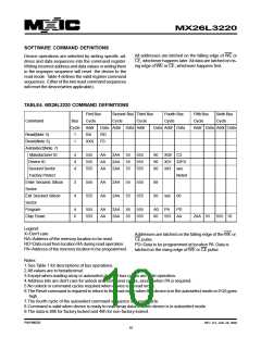
TABLE 5. SILICON ID CODE
Pins
A0 A1 A6 Q15 Q7
Q6
Q5
Q4 Q3 Q2 Q1 Q0 Code(Hex)
|
Q8
Manufacturecode
VIL VIL VIL 00H
1
1
1
1
0
1
0
1
0
1
0
1
1
0
0
1
00C2H
22FDH
Device code for MX26L3220 VIH VIL VIL 22H
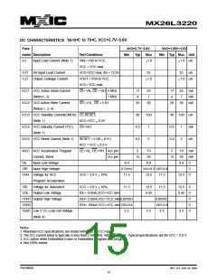
sections describe the functions of these bits. Q7, and
Q6 each offer a method for determining whether a pro-
gram or erase operation is complete or in progress.These
three bits are discussed first.
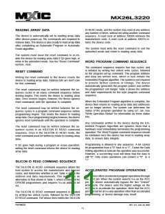
WRITE OPERSTION STATUS
The device provides several bits to determine the sta-
tus of a write operation: Q5, Q6, Q7.The following sub-
Table 6. Write Operation Status
Status
Q7
Q6
Q5
Note1
Toggle
Toggle
Toggle
Toggle
In Progress Word Program in Auto Program Algorithm
Auto Erase Algorithm
Q7
0
0
0
1
1
Exceeded
Time Limits Auto Erase Algorithm
Notes:
Word Program in Auto Program Algorithm
Q7
0
1.Performing successive read operations from any address will cause Q6 to toggle.
P/N:PM0826
REV. 0.5, JAN. 29, 2002
12

 Macronix [ MACRONIX INTERNATIONAL ]