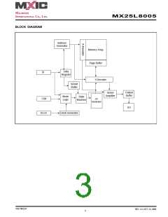
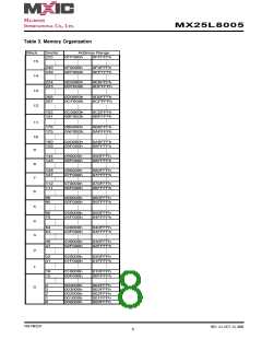
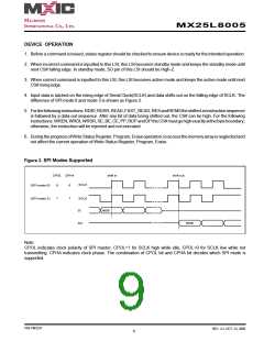
MX25L8005
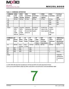
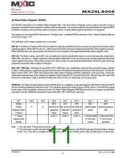
Table 2. COMMAND DEFINITION
COMMAND WREN
WRDI
(write
RDID
RDSR
WRSR
READ
FastRead
(fastread
data)
(byte)
(write
(readident- (readstatus
(writestatus (readdata)
register)
Enable)
06 Hex
disable) ification)
04 Hex 9F Hex
register)
1st
05 Hex
01 Hex
03 Hex
AD1
0B Hex
AD1
2nd
3rd
AD2
AD2
4th
AD3
AD3
5th
x
Action
sets the
(WEL)
write
reset the output the
to read out
to write new
n bytes
(WEL)
write
manufacturer the status
ID and 2-byte register
device ID
values to the readout
status register until
CS# goes
enable
latch bit
enable
latch bit
high
COMMAND SE
BE
CE
PP
DP
RDP
RES
REMS (Read
Electronic
Manufacturer
& Device ID)
90 Hex
(byte)
(Sector
(Block
Erase)
(Chip
Erase)
(Page
(Deep
(Release
(Read
Electronic
ID)
Erase)
Program) Power
Down)
fromDeep
Power-down)
1st
20 Hex
52 or
60 or
02 Hex
B9 Hex AB Hex
AB Hex
D8 Hex C7 Hex
2nd
3rd
AD1
AD2
AD3
AD1
AD2
AD3
AD1
AD2
AD3
x
x
x
x
x
4th
ADD(1)
5th
Action
Output the
manufacturer
ID and device
ID
(1) ADD=00H will output the manufacturer's ID first and ADD=01H will output device ID first.
(2) It is not recommended to adopt any other code which is not in the above command definition table.
P/N:PM1237
REV. 2.2, OCT. 23, 2008
7

 Macronix [ MACRONIX INTERNATIONAL ]