MX25L8005
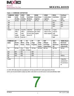
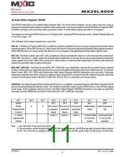
(4) Read Status Register (RDSR)
The RDSR instruction is for reading Status Register Bits. The Read Status Register can be read at any time (even in
program/erase/writestatusregistercondition)andcontinuously. ItisrecommendedtochecktheWriteinProgress(WIP)
bit before sending a new instruction when a program, erase, or write status register operation is in progress.
ThesequenceofissuingRDSRinstructionis:CS#goeslow->sendingRDSRinstructioncode->StatusRegisterdataout
on SO (see Figure. 14)
The definition of the status register bits is as below:
WIP bit. TheWriteinProgress(WIP)bit, avolatilebit, indicateswhetherthedeviceisbusyinprogram/erase/writestatus
registerprogress.WhenWIPbitsetsto1,whichmeansthedeviceisbusyinprogram/erase/writestatusregisterprogress.
When WIP bit sets to 0, which means the device is not in progress of program/erase/write status register cycle.
WELbit.TheWriteEnableLatch(WEL)bit, avolatilebit, indicateswhetherthedeviceissettointernalwriteenablelatch.
When WEL bit sets to 1, which means the internal write enable latch is set, the device can accept program/erase/write
status register instruction. When WEL bit sets to 0, which means no internal write enable latch; the device will not accept
program/erase/writestatusregisterinstruction.
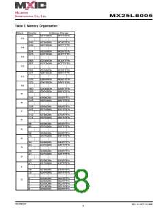
BP2, BP1, BP0 bits. The Block Protect (BP2, BP1, BP0) bits, non-volatile bits, indicate the protected area(as defined
intable1)ofthedevicetoagainsttheprogram/eraseinstructionwithouthardwareprotectionmodebeingset.Towritethe
Block Protect (BP2, BP1, BP0) bits requires the Write Status Register (WRSR) instruction to be executed. Those bits
define the protected area of the memory to against Page Program (PP), Sector Erase (SE), Block Erase (BE) and Chip
Erase(CE) instructions (only if all Block Protect bits set to 0, the CE instruction can be executed)
SRWDbit.TheStatusRegisterWriteDisable(SRWD)bit,non-volatilebit,isoperatedtogetherwithWriteProtection(WP#)
pinforprovidinghardwareprotectionmode. ThehardwareprotectionmoderequiresSRWDsetsto1andWP#pinsignal
is low stage. In the hardware protection mode, the Write Status Register (WRSR) instruction is no longer accepted for
execution and the SRWD bit and Block Protect bits (BP2, BP1, BP0) are read only.
bit 7
SRWD
bit 6
0
bit 5
0
bit 4
BP2
bit 3
BP1
bit 2
BP0
bit 1
bit 0
WIP
WEL
Status
the level of the level of the level of
(writeenable (writeinprogress
latch) bit)
RegisterWrite
Protect
protected
block
protected
block
protected
block
1= status
registerwrite
disable
(note1)
(note1)
(note1)
1=writeenable 1=writeoperation
0=notwrite
enable
0=not in write
operation
Note: 1. See the table "Protected Area Sizes".
2. Theendurancecyclesofprotectbitsare100,000cycles;however, thetWtimeoutspecofprotectbitsisrelaxed
as tW = N x 15ms (N is a multiple of 10,000 cycles, ex. N = 2 for 20,000 cycles) after 10,000 cycles on those bits.
P/N:PM1237
REV. 2.2, OCT. 23, 2008
11

 Macronix [ MACRONIX INTERNATIONAL ]