MX25L12835F
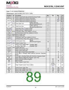
Table 17. AC CHARACTERISTICS
(Temperature = -40 C to 85 C, VCC = 2.7V ~ 3.6V)
°
°
Symbol Alt. Parameter
Min.
Typ.
Max. Unit
fSCLK
fRSCLK
fC Clock Frequency for all commands (except Read)
D.C.
133
50
MHz
MHz
MHz
MHz
ns
ns
ns
ns
V/ns
V/ns
ns
ns
ns
fR Clock Frequency for READ instructions
fT Clock Frequency for 2READ instructions
fQ Clock Frequency for 4READ instructions
84(7)
84(7)
fTSCLK
tCH(1)
Others (fSCLK)
Normal Read (fRSCLK)
Others (fSCLK)
3.3
9
3.3
9
0.1
0.1
5
tCLH Clock High Time
tCL(1)
tCLL Clock Low Time
Normal Read (fRSCLK)
tCLCH(2)
tCHCL(2)
Clock Rise Time (3) (peak to peak)
Clock Fall Time (3) (peak to peak)
tSLCH tCSS CS# Active Setup Time (relative to SCLK)
tCHSL CS# Not Active Hold Time (relative to SCLK)
tDVCH tDSU Data In Setup Time
7
2
tCHDX
tCHSH
tSHCH
tDH Data In Hold Time
3
5
5
7
ns
ns
ns
ns
ns
ns
ns
ns
ns
ns
ns
us
CS# Active Hold Time (relative to SCLK)
CS# Not Active Setup Time (relative to SCLK)
Read
tSHSL(3) tCSH CS# Deselect Time
Write/Erase/Program
30
tSHQZ(2) tDIS Output Disable Time
8
8
6
Loading: 30pF
Loading: 15pF
Clock Low to Output Valid
tCLQV
tV
Loading: 30pF/15pF
tHO Output Hold Time
Write Protect Setup Time
Write Protect Hold Time
tCLQX
tWHSL
tSHWL
tDP(2)
1
20
100
CS# High to Deep Power-down Mode
CS# High to Standby Mode without Electronic Signature
Read
CS# High to Standby Mode with Electronic Signature Read
Write Status/Configuration Register Cycle Time
Write Extended Address Register
Byte-Program
10
30
tRES1(2)
us
tRES2(2)
tW
tWREAW
tBP
30
40
us
ms
ns
us
ms
40
12
0.6
30
3
tPP
Page Program Cycle Time
0.008+
tPP(5)
Page Program Cycle Time (n bytes)
(nx0.004)
3
ms
(6)
tSE
tBE32
tBE
Sector Erase Cycle Time
43
190
340
72
200
1000
2000
160
ms
ms
ms
s
Block Erase (32KB) Cycle Time
Block Erase (64KB) Cycle Time
Chip Erase Cycle Time
tCE
P/N: PM1795
REV. 1.0, OCT. 23, 2012
89

 Macronix [ MACRONIX INTERNATIONAL ]