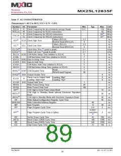
MX25L12835F
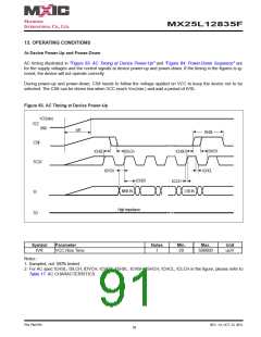
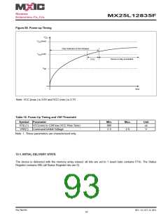
Figure 85. Power-up Timing
V
CC
V
(max)
CC
Chip Selection is Not Allowed
V
(min)
CC
Device is fully accessible
tVSL
V
WI
time
Note: VCC (max.) is 3.6V and VCC (min.) is 2.7V.
Table 18. Power-Up Timing and VWI Threshold
Symbol Parameter
Min.
800
2.3
Max.
Unit
us
V
tVSL(1)
VWI(1)
VCC(min) to CS# low (VCC Rise Time)
Command Inhibit Voltage
2.5
Note: 1. These parameters are characterized only.
13-1. INITIAL DELIVERY STATE
The device is delivered with the memory array erased: all bits are set to 1 (each byte contains FFh). The Status
Register contains 00h (all Status Register bits are 0).
P/N: PM1795
REV. 1.0, OCT. 23, 2012
93

 Macronix [ MACRONIX INTERNATIONAL ]